UG-1828 Preliminary Technical Data
Rev. PrC | Page 280 of 338
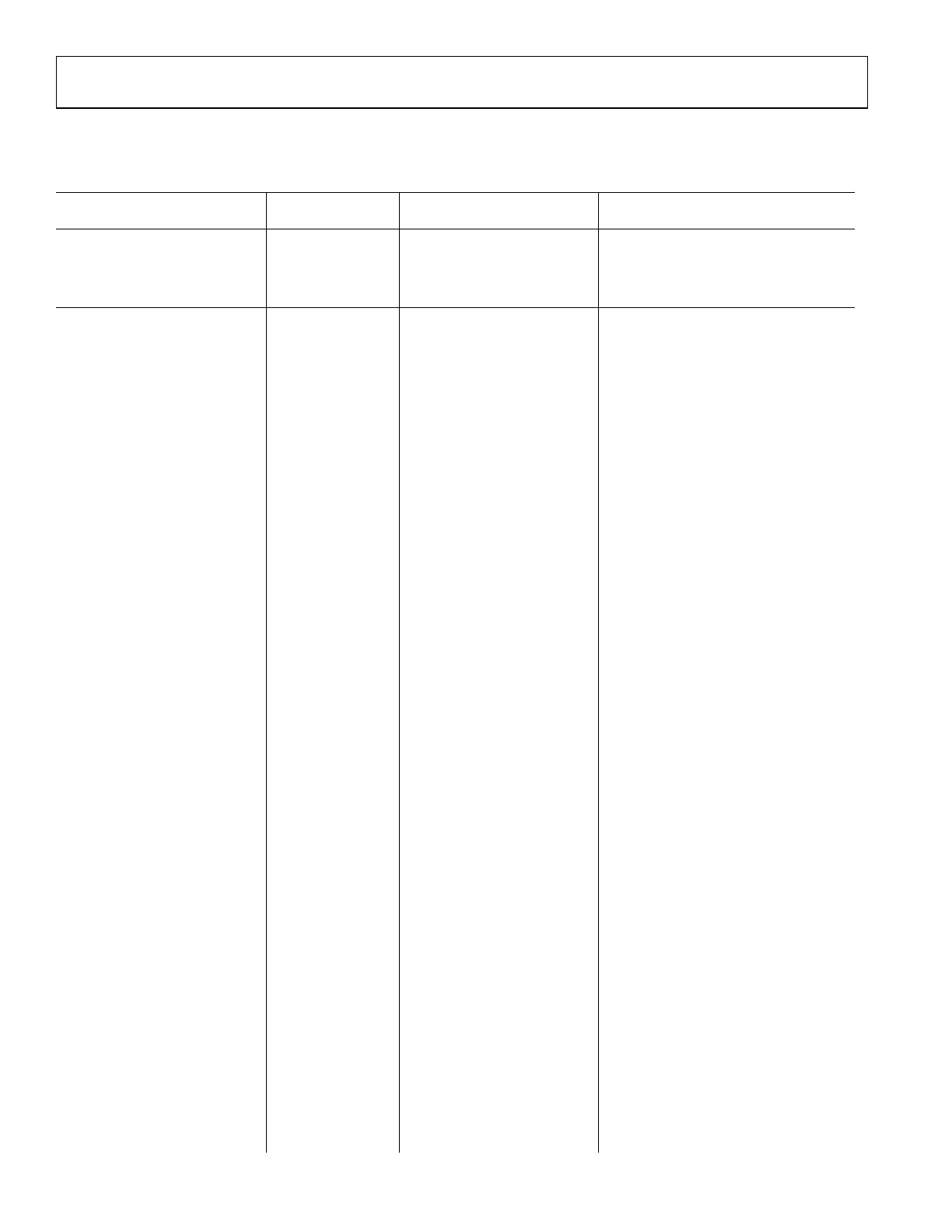
In case where not all RF IOs or other interface pins are utilized in end application user should follow Table 109 for recommendation what
to do with unused pins.
Table 109. Instruction Explaining How to Handle ADRV9001 Unused Pins
Pin No. Type Mnemonic Unused instructions
A1, A2, A13, A14, B2 to B5, B10 to
B13, C2, C5, C10, C13, D1 to D6, D9
to D14, E6, E9, F1 to F3, F6 to F9,
F12 to F14, G2, G13, J1 to J14,
Input VSSA Not applicable.
A3, A4 Input EXT_LO2+, EXT_LO2− Connect to VSSA.
A5 Input VRFVCO2_1P3 Connect to VSSA when unused
A6 Input/Output VRFLO2_1P0 Not applicable.
A7 Input MODEA Not applicable.
A8 Input RBIAS Not applicable.
A9 Input/Output VRFLO1_1P0 Not applicable.
A10 Input VRFVCO1_1P3 Connect to VSSA when unused
B1, C1 Input RX2A-, RX2A+ When accidentally enabled, bias voltage
could be present on those inputs.
Connect to VSSA thru capacitor.
B6 Output VRFVCO2_1P0 Connect to VSSA when unused
B7 Input AUXADC_2 Do not connect.
B8 Input AUXADC_1 Do not connect.
B9 Output VRFVCO1_1P0 Connect to VSSA when unused
B14, C14 Input RX1A-, RX1A+ When accidentally enabled, bias voltage
could be present on those inputs.
Connect to VSSA thru capacitor.
C3, C4 Input RX2B+, RX2B- When accidentally enabled, bias voltage
could be present on those inputs.
Connect to VSSA thru capacitor
C6 Input/Output VANA2_1P0 Connect to VSSA when unused
C7 Input VANA2_1P3 Connect to VSSA when unused
C8 Input VANA1_1P3 Not applicable.
C9 Input/Output VANA1_1P0 Not applicable.
C11, C12 Input RX1B-, RX1B+ When accidentally enabled, bias voltage
could be present on those inputs.
Connect to VSSA thru capacitor.
D7, D8 Input MCS+, MCS- Connect to VSSA.
E1 Output VRX2LO_1P0 Connect to VSSA when unused
E2 Input VRX2LO_1P3 Connect to VSSA when unused
E3, E12, F4, F5, F10, F11, G4, G6, G9,
G11, H6, H9
Input/Output AGPIO_xx Do not connect.
E4 Input VRFSYN2_1P3 Connect to VSSA when unused
E5 Input VCLKSYN_1P3 Not applicable.
E10 Input VAUXSYN_1P3 Not applicable.
E11 Input VRFSYN1_1P3 Connect to VSSA when unused
E13 Input VRX1LO_1P3 Not applicable.
E14 Output VRX1LO_1P0 Not applicable.
G1, H1 Output TX2+, TX2- Do not connect.
G3 Input VTX2LO_1P3 Connect to VSSA when unused
G5 Input VCLKVCO_1P3 Not applicable.
 Loading...