Preliminary Technical Data UG-1828
Rev. PrC | Page 311 of 338
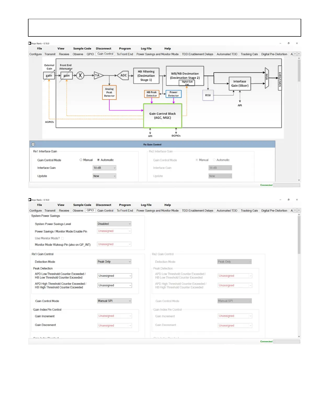
Figure 295. Rx Gain Control Tab
Figure 296. GPIO Configuration
For more detailed information refer to Rx Gain Control section of this document. The GPIO tab also shares a section with the frequency
hopping as seen in Figure 285.
Tx Front End
Tx Attenuation
 Loading...