UG-1828 Preliminary Technical Data
Rev. PrC | Page 58 of 338
Figure 38. Receive CSSI timing with 8× Data Clock Rate for 16-Bit I/Q Data Sample (MSB First), 224 Cycles
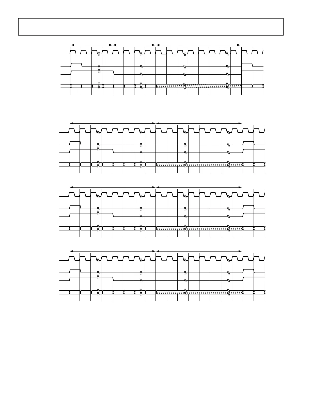
Figure 39, Figure 40, and Figure 41 illustrate the Receive CSSI interface (Rx1 and Rx2) in frequency deviation mode with 16-bit data
symbol with 2×, 4×, and 8× clock rates. The strobe pulse validates the start of the 16bits data symbol, the remaining data bits are ignored.
Figure 39. Receive CSSI Timing with 2× Data Clock Rate for 16-Bit Data Symbol (MSB First)
Figure 40. CSSI Receive Timing with 4× Data Clock Rate for 16-Bit Data Symbol (MSB First)
Figure 41. Receive CSSI Timing with 8× Data Clock Rate for 16-Bit Data Symbol (MSB First)
Four-Lane Mode CSSI Interface
The four-lane mode receive CSSI interface of each channel (Rx1 and Rx2) are a 6-wire digital interface consisting of:
• RX_DCLK_OUT: is an output clock synchronous data and strobe output signals.
• RX_STROBE_OUT: is an output signal indicating the first bit of the serial data sample.
• RX_IDATA0_OUT: is an output serial data stream of I sample low byte.
• RX_IDATA1_OUT: is an output serial data stream of I sample high byte.
• RX_QDATA2_OUT: is an output serial data stream of Q sample low byte.
• RX_QDATA3_OUT: is an output serial data stream of Q sample high byte.
Figure 42 illustrates the receive CSSI interface (Rx1 and Rx2) for a four-lane format with MSB first configuration.
RX_DCLK_OUT
RX_STROBE_OUT
OR
RX_STROBE_OUT
RX_DATA_OUT
16 CYCLES (I SAMPLE)
16 CYCLES (Q SAMPLE)
224 CYCLES (NO SAMPLE)
I0_D15 I0_D14 I0_D0 Q0_D15 Q0_D14 Q0_D0 I0_D14I1_D15
24159-035
RX_CLOCK_OUT
RX_STROBE_OUT
OR
RX_STROBE_OUT
RX_DATA_OUT
16 CYCLES (I SAMPLE)
16 CYCLES (NO SAMPLE)
I0_D15 I0_D14
I0_D8 I0_D7 I0_D6 I0_D0 I0_D14
I1_D15
24159-036
RX_CLOCK_OUT
RX_STROBE_OUT
OR
RX_STROBE_OUT
RX_DATA_OUT
16 CYCLES (I SAMPLE) 48 CYCLES (NO SAMPLE)
I0_D15 I0_D14 I0_D8 I0_D7 I0_D6 I0_D0
I0_D14I1_D15
24159-037
RX_CLOCK_OUT
RX_STROBE_OUT
OR
RX_STROBE_OUT
RX_DATA_OUT
16 CYCLES (I SAMPLE) 112 CYCLES (NO SAMPLE)
I0_D15 I0_D14 I0_D8 I0_D7 I0_D6 I0_D0 I0_D14I1_D15
24159-038
 Loading...