UG-1828 Preliminary Technical Data
Rev. PrC | Page 60 of 338
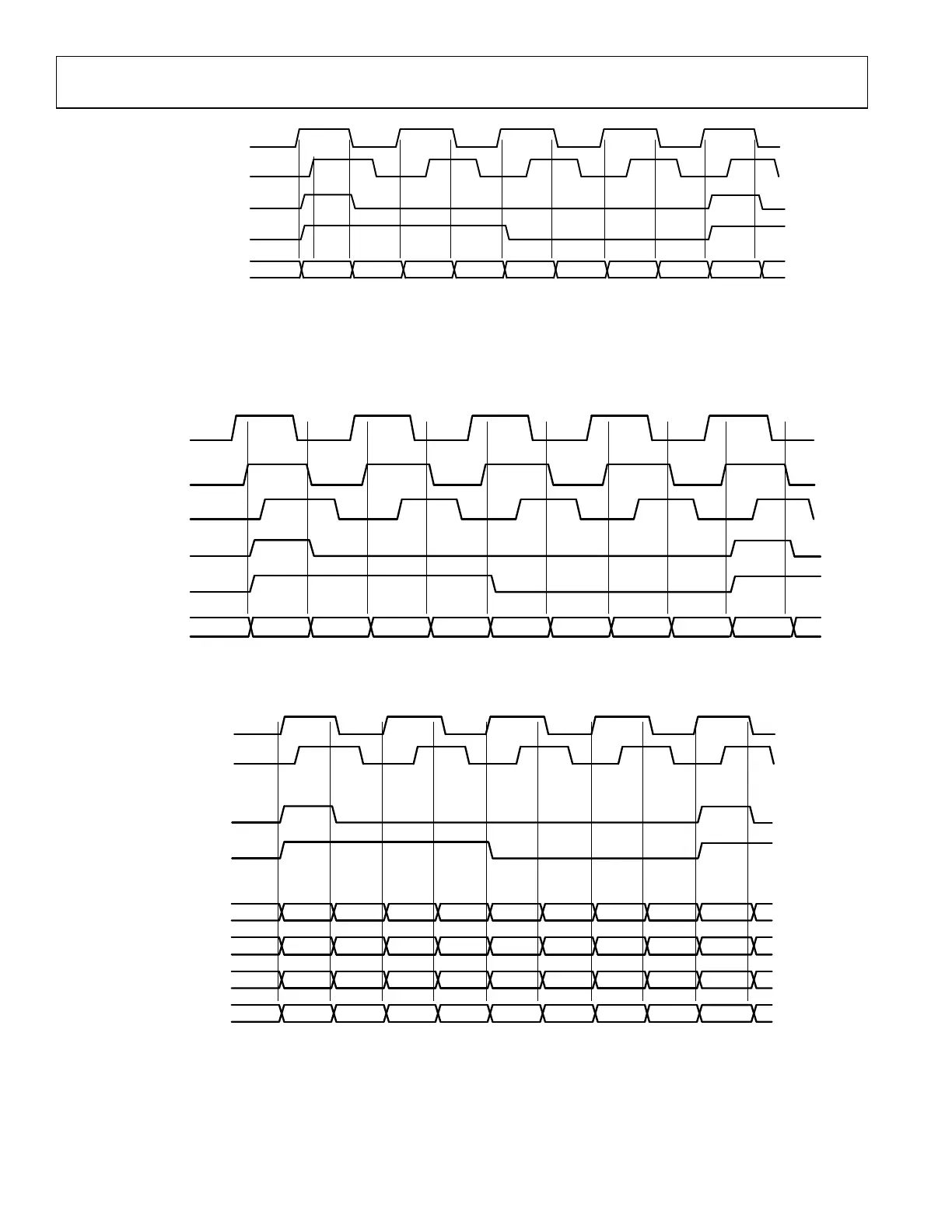
Figure 44. Receive CSSI DDR Clock Relation with Strobe/Data
Figure 45 illustrates the transmit CMOS SSI interface with DDR clock in relation with strobe/data, with respect to ADRV9001. Each edge
of the clock (positive and negative) samples the corresponding strobe/data sample based on the interface setup/hold timing.
When the baseband processor drives out the transmit SSI clock, strobe and data to ADRV9001, the output DDR clock can be in-phase
with the strobe/data or delayed quarter cycle of the clock period, it’s up to the user, but the relation between transmit DDR clock and
strobe/data must meet the ADRV9001 setup and hold timing specification.
Figure 45. Transmit CSSI DDR Clock Relation with Strobe/Data
Figure 46 and Figure 46 illustrate the timing diagram example for four-lane mode receive, transmit CSSI with DDR clock, 16-bit I/Q
sample.
Figure 46. Four-Lane Mode Receive CSSI DDR Timing for 16-Bit I/Q Data Sample
RX_DCLK_OUT
OR
RX_DCLK_OUT
WITH QUARTER CLOCK
CYCLE DELAY
(OPTIONAL)
RX_STROBE_OUT
OR
RX_STROBE_OUT
RX_IDATA_IN
I0_D15 I0_D14 I0_D8 I0_D7 I0_D6 I0_D0 I1_D15
24159-041
TX_DCLK_IN
OR
TX_DCLK_IN
TX_DCLK_OUT
TX_STROBE_IN
OR
TX_STROBE_IN
TX_IDATA_IN
I0_D15 I0_D14
I0_D8 I0_D7
I0_D6
I0_D0 I1_D15
24159-042
RX_IDATA0_IN
RX_DCLK_OUT
OR
RX_DCLK_OUT
RX_STROBE_OUT
OR
RX_STROBE_OUT
I0_D7 I0_D6 I0_D5 I0_D4 I0_D3 I0_D2 I0_D1 I0_D0 I1_D7
RX_IDATA1_IN
I0_D15 I0_D14 I0_D13 I0_D12 I0_D11 I0_D10 I0_D9 I0_D8 I1_D15
RX_QDATA2_IN
Q0_D7 Q0_D6 Q0_D5 Q0_D4 Q0_D3 Q0_D2 Q0_D1 Q0_D0 Q1_D7
RX_QDATA3_IN
Q0_D15 Q0_D14 Q0_D13 Q0_D12 Q0_D11 Q0_D10 Q0_D9 Q0_D8 Q1_D15
24159-043
 Loading...