Preliminary Technical Data UG-1828
Rev. PrC | Page 67 of 338
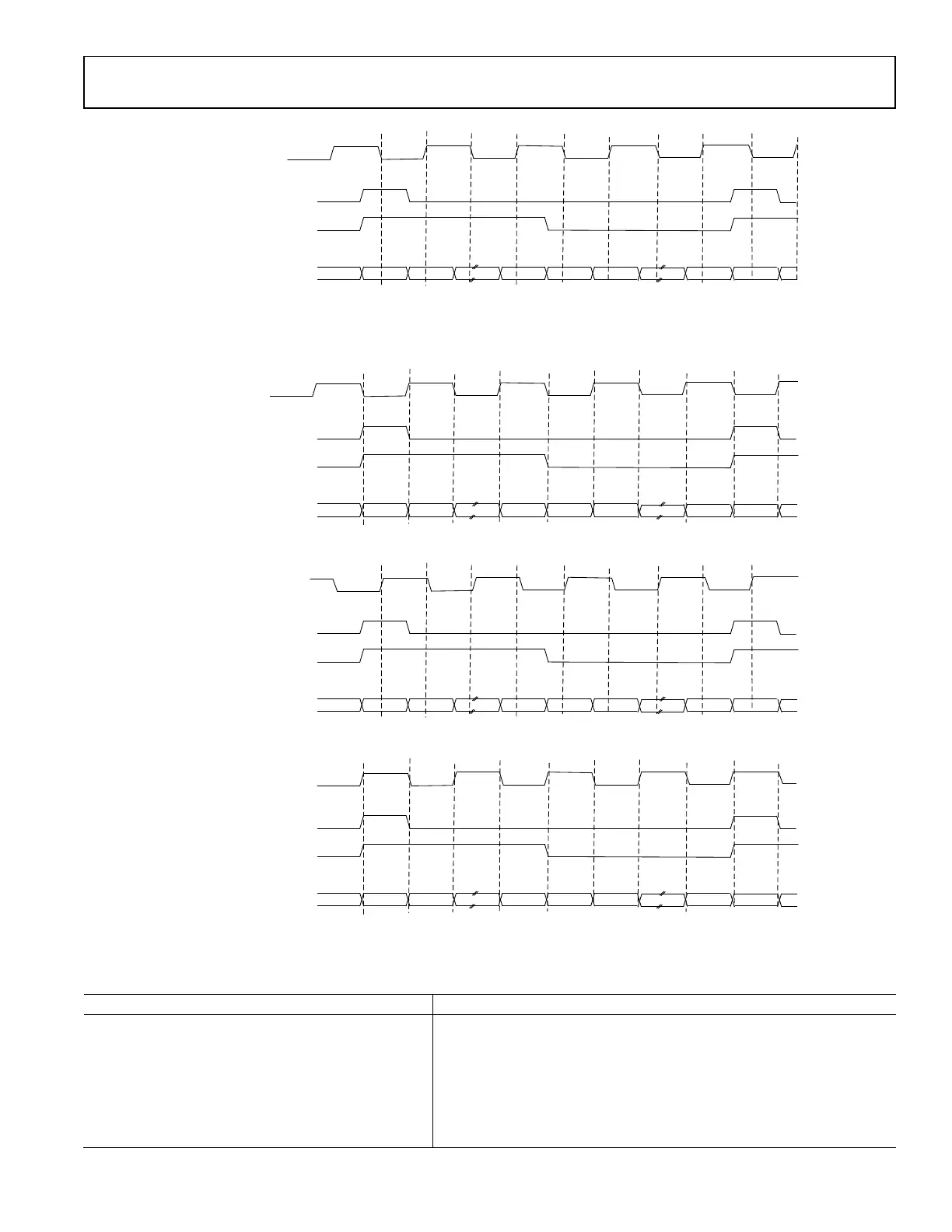
RX_IDATA_OUT
I0_D15
RX_STROBE_OUT
I0_D0
I0_D14
I0_D7
I0_D6
RX_STROBE_OUT
I0_D8
I1_D15
Rx_DCLK_OUT
Or
Figure 56 RX CMOS DDR SSI Default(Recommend) output (cmosDdrPosClkEn=False, cmosClkInversionEn=False)
Users can also manually edit the CMOS DDR relative configurations based on their BBIC requirements, Figure 57, Figure 58, Figure 59
shows the corresponding Rx output Clock/Strobe/Data timing diagram with different CMOS DDR configuration.
RX_IDATA_OUT
I0_D15
RX_STROBE_OUT
I0_D0
I0_D14
I0_D7
I0_D6
RX_STROBE_OUT
I0_D8
I1_D15
Rx_DCLK_OUT
Or
Figure 57 RX CMOS DDR SSI output (cmosDdrPosClkEn=True, cmosClkInversionEn=False)
RX_IDATA_OUT
I0_D15
RX_STROBE_OUT
I0_D0
I0_D14
I0_D7
I0_D6
RX_STROBE_OUT
I0_D8
I1_D15
Rx_DCLK_OUT
Or
Figure 58 RX CMOS DDR SSI output (cmosDdrPosClkEn=False, cmosClkInversionEn=True)
RX_IDATA_OUT
I0_D15
RX_STROBE_OUT
I0_D0
I0_D14
I0_D7
I0_D6
RX_STROBE_OUT
I0_D8
I1_D15
Rx_DCLK_OUT
Or
Figure 59 RX CMOS DDR SSI output (cmosDdrPosClkEn=True, cmosClkInversionEn=True)
A set of API commands are provided to set and inspect the SSI test/debug functions, which are summarized in Table 21.
Table 21. SSI Test/Debug API List
SSI Function Name Description
adi_adrv9001_Ssi_Rx_TestMode_Configure Configures the SSI test mode for the specified Rx channel
adi_adrv9001_Ssi_Tx_TestMode_Configure Configures the SSI test mode for the specified Tx channel
adi_adrv9001_Ssi_Tx_TestMode_Status_Inspect Inspects the SSI test mode status for the specified Tx channel
adi_adrv9001_Ssi_Loopback_Set Set the enabledness of Rx to Tx SSI interface loopback
adi_adrv9001_Ssi_Delay_Configure
Programs the SSI delay configuration
adi_adrv9001_Ssi_Delay_Inspect Gets the SSI delay configuration from ADRV9001 device
adi_adrv9001_Ssi_PowerDown_Set Set the power down mode for the specified channel and SSI type
 Loading...