Chapter 1 — General Information 1-6 MN469xC Multiport Test Set Functional Description
MN469xC Series Multiport Test Set MM PN: 10410-00730 Rev. D 1-5
1-6 MN469xC Multiport Test Set Functional Description
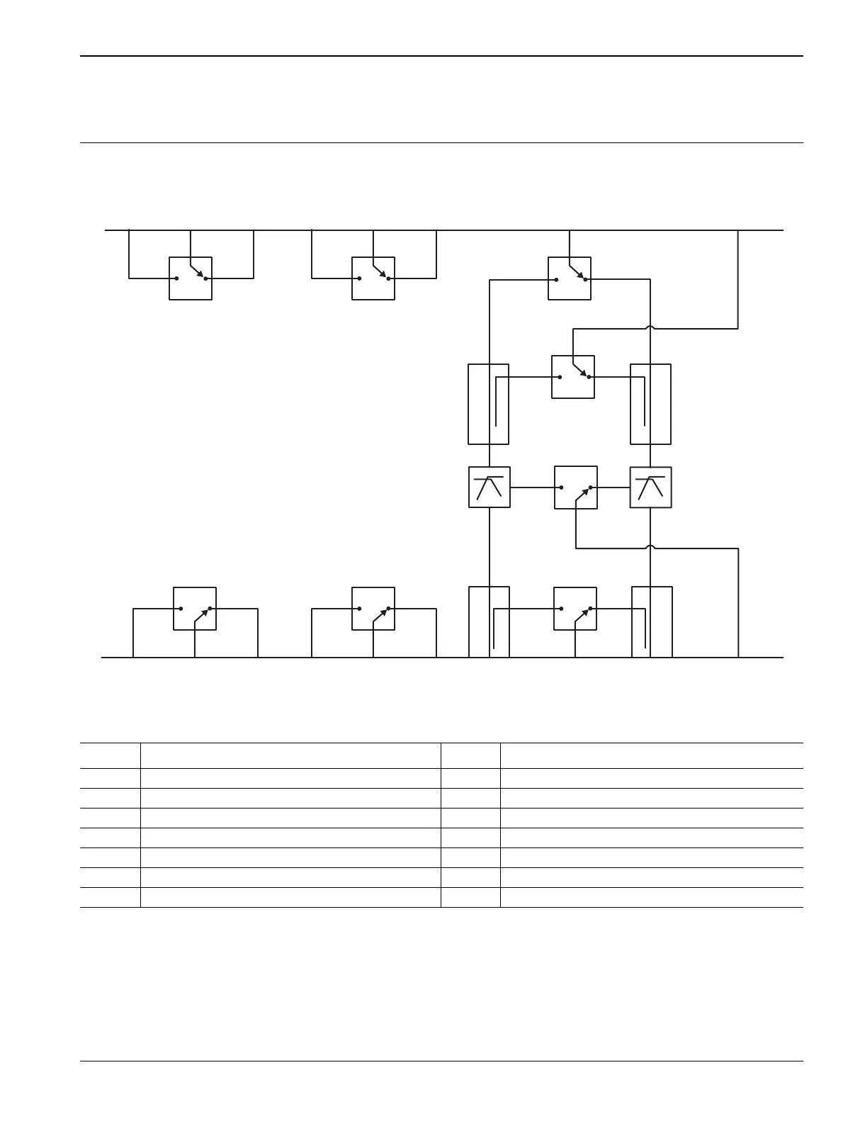
A block diagram of the MN469xC Series Multiport Test Set is shown in Figure 1-2.
The VectorStar VNA sends switch control commands via the GPIB bus to the GPIB to Parallel Digital
Interface PCB Assembly in the test set. The logic in this PCB is translated by the 4-Port Test Set Control PCB
to the appropriate levels at any given time to control each one of the SPDT RF switches in the test set.
Module Description Module Description
A4 Low Band Switch A13 High Band SPDT Switch
A5 Low Band Switch A14 Port Coupler
A6 Low Band Switch A15 Port Coupler
A7 Low Band Switch A18 High Band SPDT Switch
A8 Diplexer/Bias-Tee A19 High Band SPDT Switch
A10 Diplexer/Bias-Tee A20 Low Band Bridge
A12 High Band SPDT Switch A21 Low Band Bridge
Figure 1-2. MN469xC Functional Block Diagram
Pt 1 Src
Input
Pt 1 Src
Output
b1
Out
b2
Out
Pt 2 Src
Input
Pt 1 Src
Input
Pt 1 Src
Output
Pt 2 Src
Input
A19 A13
A15
A18
A5
A4
A20 A21
A10A8
A7A6
A12
A14
b1
Input
b1
Out
b2
Out
Port 3 Port 4
b1
Input
To VNA
Port 2 Source
Output
To VNA
Port 2 Source
Output
To VNA
b2
Input
To VNA
b2
Input
(REAR PANEL)
(FRONT PANEL)
 Loading...