LDM41A and LDM42A Manual Content
ASTECH GmbH Page 5
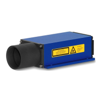
II. List of Figures
Figure 1 : Measurement principle ...................................................................... 7
Figure 2 : Warning Sign Laser Radiation Class 2 ............................................... 10
Figure 3 : Dimensional drawing ........................................................................ 14
Figure 4 : Offset against zero-edge ................................................................... 15
Figure 5 : View of LDM41A and LDM42A pole assignments ............................. 16
Figure 6 : Interface cable with connector ......................................................... 17
Figure 7 : Interface cable color codes ............................................................... 17
Figure 8 : Isolated Mounting ............................................................................. 19
Figure 9 : Recommended terminations wiring for work with open RS-232 ..... 20
Figure 10 : Program LDMTool ........................................................................... 22
Figure 11 : Help text Firmware V7.x ................................................................. 24
Figure 12 : Help text Firmware V8.x ................................................................. 25
Figure 13 : Trigger level = 1 ............................................................................... 38
Figure 14 : Trigger level = 0 ............................................................................... 38
Figure 15 : Diagram of RS232 wiring at 9-position D-Sub cable jack ................ 41
Figure 16 : Diagram of RS232 wiring at 25-pole D-Sub cable jack .................... 41
Figure 17 : RS232 wiring diagram ..................................................................... 42
Figure 18 : Wiring diagram of digital switching output .................................... 43
Figure 19 : Digital switching output behavior ................................................... 44
Figure 20 : Wiring diagram of analog output .................................................... 45
Figure 21 :Output current diagram for RE > RB and RE < RB ............................ 46
Figure 22 : Wiring diagram of trigger input ...................................................... 47
Figure 23 : RS232 cable with power supply for LDM41A and LDM42A ............ 51