AT90S4414/8515
16
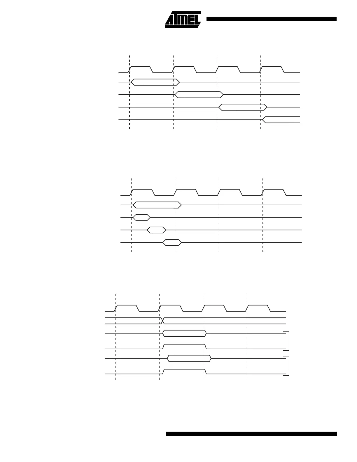
Figure 20. The Parallel Instruction Fetches and Instruction Executions
Figure 21 shows the internal timing concept for the register file. In a single clock cycle an ALU operation using two register
operands is executed, and the result is stored back to the destination register.
Figure 21. Single Cycle ALU Operation
The internal data SRAM access is performed in two System Clock cycles as described in Figure 22.
Figure 22. On-chip Data SRAM Access Cycles
See “Interface to External SRAM” on page 53 for a description of the access to the external SRAM.
System Clock Ø
1st Instruction Fetch
1st Instruction Execute
2nd Instruction Fetch
2nd Instruction Execute
3rd Instruction Fetch
3rd Instruction Execute
4th Instruction Fetch
T1 T2 T3 T4
System Clock Ø
Total Execution Time
Register Operands Fetch
ALU Operation Execute
Result Write Back
T1 T2 T3 T4
System Clock Ø
WR
RD
Data
Data
Address
Address
T1 T2 T3 T4
Prev. Address
Read Write

 Loading...


