126
7679H–CAN–08/08
AT90CAN32/64/128
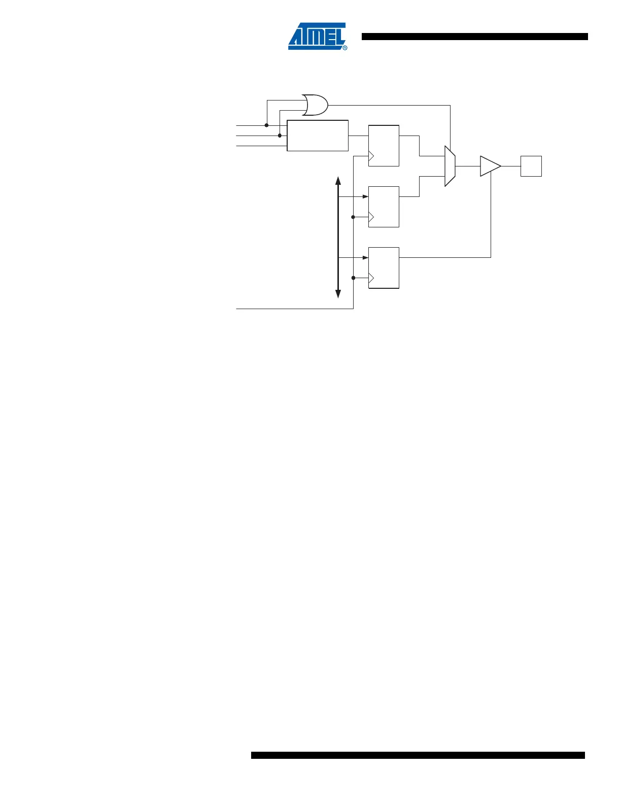
Figure 13-5. Compare Match Output Unit, Schematic
13.8.1 Compare Output Function
The general I/O port function is overridden by the Output Compare (OCnx) from the Waveform
Generator if either of the COMnx1:0 bits are set. However, the OCnx pin direction (input or out-
put) is still controlled by the Data Direction Register (DDR) for the port pin. The Data Direction
Register bit for the OCnx pin (DDR_OCnx) must be set as output before the OCnx value is visi-
ble on the pin. The port override function is generally independent of the Waveform Generation
mode, but there are some exceptions. Refer to Table 13-1, Table 13-2 and Table 13-3 for
details.
The design of the Output Compare pin logic allows initialization of the OCnx state before the out-
put is enabled. Note that some COMnx1:0 bit settings are reserved for certain modes of
operation. See “16-bit Timer/Counter Register Description” on page 135.
The COMnx1:0 bits have no effect on the Input Capture unit.
13.8.2 Compare Output Mode and Waveform Generation
The Waveform Generator uses the COMnx1:0 bits differently in normal, CTC, and PWM modes.
For all modes, setting the COMnx1:0 = 0 tells the Waveform Generator that no action on the
OCnx Register is to be performed on the next compare match. For compare output actions in the
non-PWM modes refer to Table 13-1 on page 136. For fast PWM mode refer to Table 13-2 on
page 136, and for phase correct and phase and frequency correct PWM refer to Table 13-3 on
page 137.
A change of the COMnx1:0 bits state will have effect at the first compare match after the bits are
written. For non-PWM modes, the action can be forced to have immediate effect by using the
FOCnx strobe bits.
13.9 Modes of Operation
The mode of operation, i.e., the behavior of the Timer/Counter and the Output Compare pins, is
defined by the combination of the Waveform Generation mode (WGMn3:0) and Compare Output
mode (COMnx1:0) bits. The Compare Output mode bits do not affect the counting sequence,
PORT
DDR
DQ
DQ
OCnx
Pin
OCnx
DQ
Waveform
Generator
COMnx1
COMnx0
0
1
DATA BUS
FOCnx
clk
I/O

 Loading...


