311
7679H–CAN–08/08
AT90CAN32/64/128
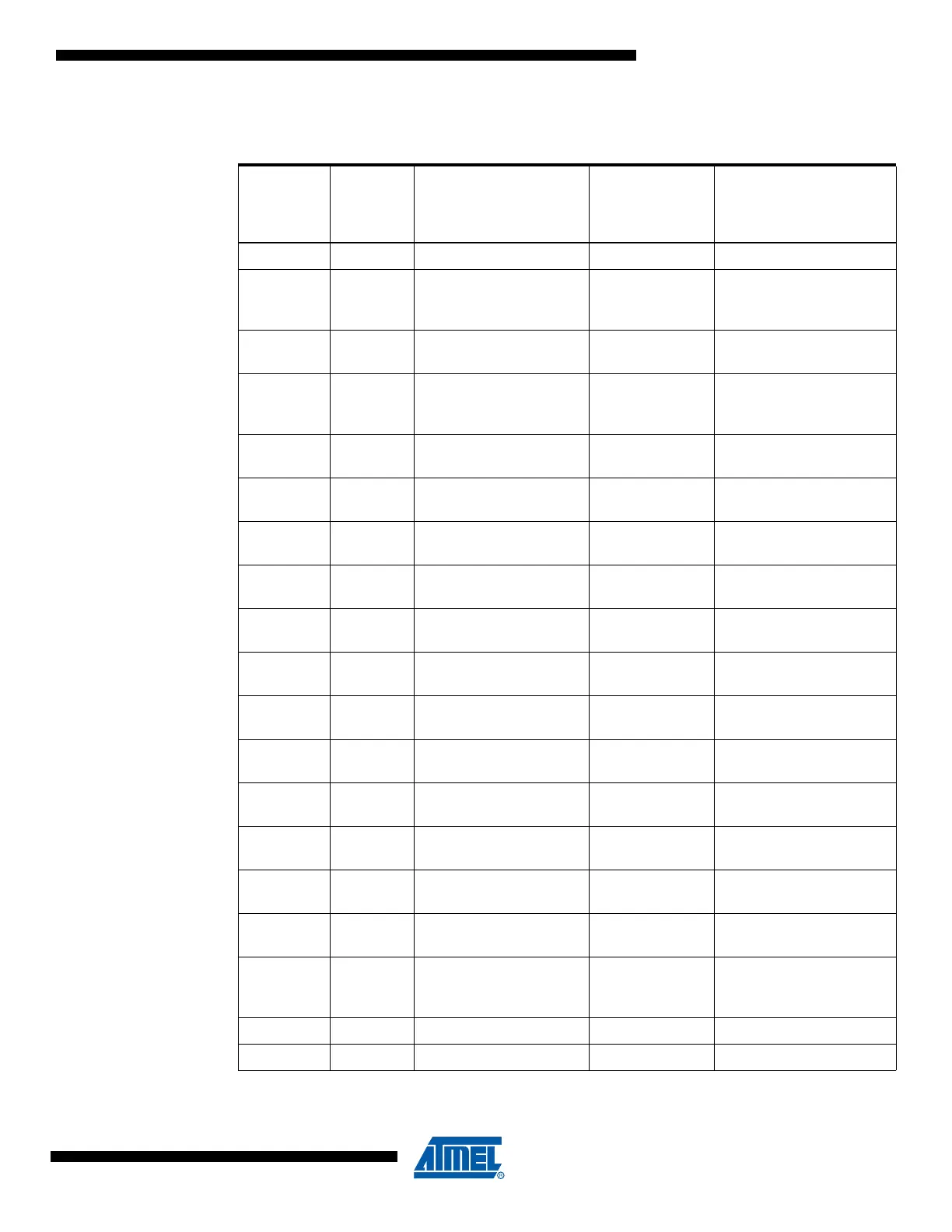
Table 23-7. Boundary-scan Signals for the ADC
(1)
Signal
Name
Direction
as Seen
from the
ADC
Description
Recommended
Input
when not in use
Output Values when
Recommended Inputs
are Used, and CPU is
not Using the ADC
COMP Output Comparator Output 0 0
ACLK Input
Clock signal to gain
stages implemented as
Switch-cap filters
00
ACTEN Input
Enable path from gain
stages to the comparator
00
ADCBGEN Input
Enable Band-gap
reference as negative
input to comparator
00
ADCEN Input
Power-on signal to the
ADC
00
AMPEN Input
Power-on signal to the
gain stages
00
DAC_9 Input
Bit 9 of digital value to
DAC
11
DAC_8 Input
Bit 8 of digital value to
DAC
00
DAC_7 Input
Bit 7 of digital value to
DAC
00
DAC_6 Input
Bit 6 of digital value to
DAC
00
DAC_5 Input
Bit 5 of digital value to
DAC
00
DAC_4 Input
Bit 4 of digital value to
DAC
00
DAC_3 Input
Bit 3 of digital value to
DAC
00
DAC_2 Input
Bit 2 of digital value to
DAC
00
DAC_1 Input
Bit 1 of digital value to
DAC
00
DAC_0 Input
Bit 0 of digital value to
DAC
00
EXTCH Input
Connect ADC channels 0
- 3 to by-pass path
around gain stages
11
G10 Input Enable 10x gain 0 0
G20 Input Enable 20x gain 0 0

 Loading...


