340
7679H–CAN–08/08
AT90CAN32/64/128
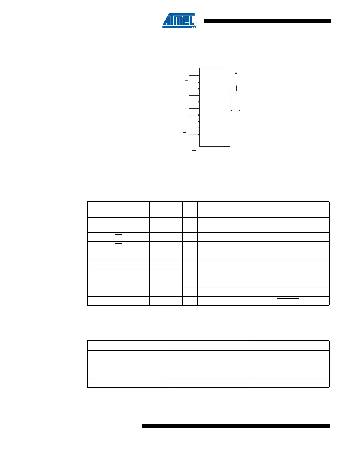
Figure 25-1. Parallel Programming
25.5.2 Pin Mapping
25.5.3 Commands
VCC
+2.7 - +5.5V
GND
XTAL1
PD1
PD2
PD3
PD4
PD5
PD6
PB7 - PB0
DATA
RESET
PD7
+12 V
BS1
XA0
XA1
OE
RDY/BSY
PAGEL
PA0
WR
BS2
AVCC
+2.7 - +5.5V
Table 25-7. Pin Name Mapping
Signal Name in
Programming Mode
Pin Name I/O Function
RDY/BSY PD1 O
0: Device is busy programming,
1: Device is ready for new command.
OE
PD2 I Output Enable (Active low).
WR PD3 I Write Pulse (Active low).
BS1 PD4 I Byte Select 1 (“0” selects low byte, “1” selects high byte).
XA0 PD5 I XTAL Action Bit 0
XA1 PD6 I XTAL Action Bit 1
PAGEL PD7 I Program Memory and EEPROM data Page Load.
BS2 PA0 I Byte Select 2 (“0” selects low byte, “1” selects 2’nd high byte).
DATA PB7-0 I/O Bi-directional Data bus (Output when OE is low).
Table 25-8. Pin Values Used to Enter Programming Mode
Pin Symbol Value
PAGEL Prog_enable[3] 0
XA1 Prog_enable[2] 0
XA0 Prog_enable[1] 0
BS1 Prog_enable[0] 0

 Loading...


