15
AT90S2313
0839G–08/01
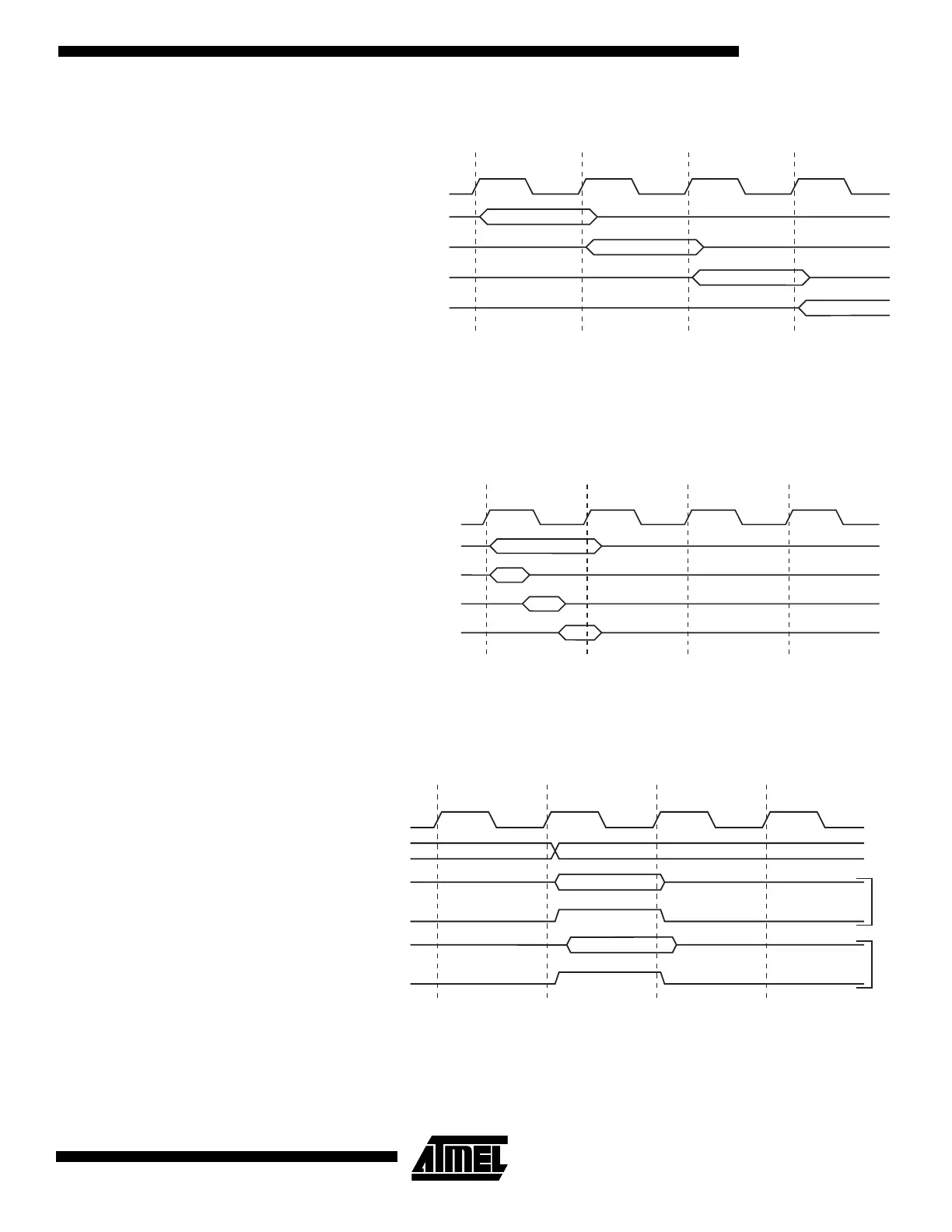
Figure 20. The Parallel Instruction Fetches and Instruction Executions
Figure 21 shows the internal timing concept for the register file. In a single clock cycle
an ALU operation using two register operands is executed, and the result is stored back
to the destination register.
Figure 21. Single-cycle ALU Operation
The internal data SRAM access is performed in two System Clock cycles as described
in Figure 22.
Figure 22. On-chip Data SRAM Access Cycles
System Clock Ø
1st Instruction Fetch
1st Instruction Execute
2nd Instruction Fetch
2nd Instruction Execute
3rd Instruction Fetch
3rd Instruction Execute
4th Instruction Fetch
T1 T2 T3 T4
System Clock Ø
Total Execution Time
Register Operands Fetch
ALU Operation Execute
Result Write Back
T1 T2 T3 T4
System Clock Ø
WR
RD
Data
Data
Address
Address
T1 T2 T3 T4
Prev. Address
Read
Write

 Loading...


