2. Working principle
(1) Realization of button function: when users are operating machine, button matrix circuit will
produce a button information, and recognise button through S0793 to produce button function code to
transmit to the main CPU inside decode chip, CPU performs the corresponding switch to the function
module inside system, and a signal will produce to control OSD and panel display part to make the
corresponding display.
(2) Panel display drive: when the serial data signals conveyed by decode chip is transmitting to
panel IC (S0793), IC performs VFD drive according to the information conveyed by decode and displays
the corresponding content (controlled by software).
(3) Panel light control light: LED2 controls power switch indicator light, and it is high level after
power on; LED1 controls open/close button indicator light, after power on, low level is outputted to
lighten VD105, square wave signal is outputted when disc out and disc reading, VD105 flashes, it is high
level when playing normally, VD105 turns out.
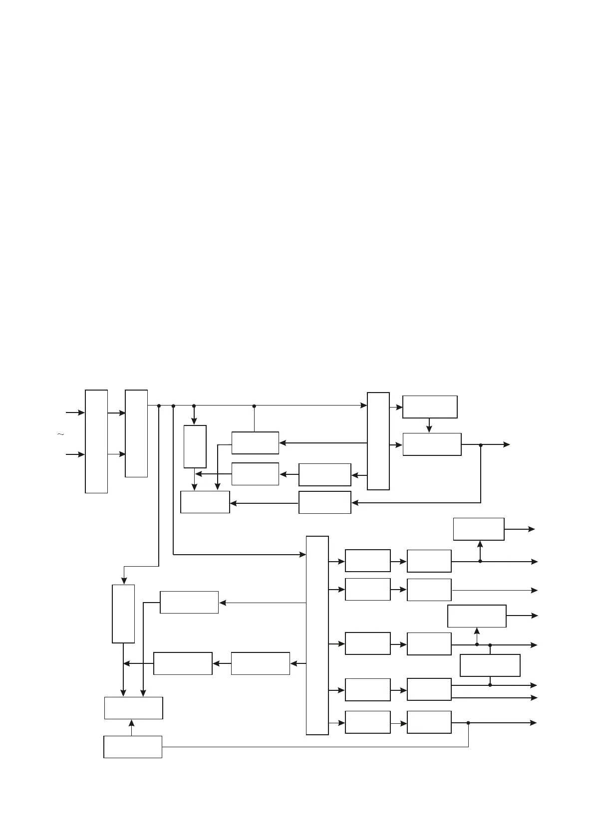
3.2.6 Power circuit
1. Power circuit block diagram is shown in the following figure 3.2.6.1:
Bridge rectification
filtering circuit
Start-up
circuit
Switch
module
Absorption
loop
Filtering
Rectification
diode
Feedback
loop
Transformer
Rectification
diode
Filtering circuit
P+28V
Start-up
circuit
Switch module
Absorption
loop
Filtering
Rectification
diode
Transformer
Feedback circuit
Rectification
circuit
Filtering
circuit
Rectification
circuit
Filtering
circuit
Rectification
circuit
Filtering
circuit
Voltage
regulating diode
5V voltage
regulator
A+5V
A+12V
D+5V
A-12V
-21V
Voltage
regulating diode
Rectification
circuit
Filtering
circuit
FL+
FL-
Rectification
circuit
Filtering
circuit
D+3V3
220V
Electromagnetic interference
filtering circuit
Figure 3.2.6.1 Power circuit block diagram
- 22 -