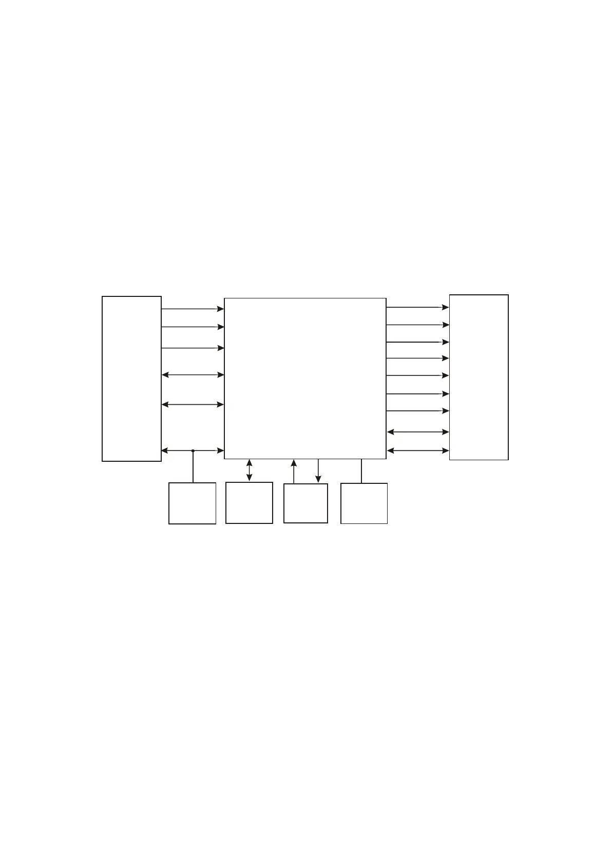
3.2.1 Decode circuit
1. Decode circuit block diagram is shown as in the following figure 3.2.1.1:
SDRAM
SDCLK
SDCKE
DCS
DRAS
SWE
DQM0
DQM1
DQ0~DQ15
MA0~MA11
URST
PWR
PRD
PCE
A0~A20
AD0~AD7
MT 1389
FLASH
EEPROM
24C02
SDA
SCL
Reset
circuit
Clock
1.8V
voltage
regulating
U206
V18
27M
Figure 3.2.1.1 Decode circuit block diagram
2. Working principle: this decode circuit is mainly composed of MT1389, SDRAM and FLASH.
Working condition of decode circuit has:
(1) Reset: refer to reset circuit working principle for details.
(2) Clock: this system adopts 27M external clock input, and produces clock signal required by
system inside through internal frequency doubling circuit.
(3) Power: decode chip adopts twp groups power supply of 3.3V and 1.8V, in which 1.8V mainly
supply power for internal logic control circuit and we call it core voltage.
After power on, reset circuit performs reset to MT1389 built-in CPU (8032) and FLASH, decode chip
outputs reset signal at the same time and performs reset to other circuit. After system reset, it firstly
sends out read signal to FLASH to read out in formation saved in FLASH, the machine displays power-
on picture, servo system begins to work to check whether machine closes door to proper position and
Section Two Unit Circuit Principle
- 16 -