- 24 -
2.5V (means output voltage is on low side), LM431 cuts off, the “on” time of VEPR22 increases, output
voltage increases, thus power board outputs stable voltage through the auto control function of
feedback loop.
(9) Filtering circuit: the function is to produce a stable and small-ripple DC voltage. “ “-style filter is
often adopted in filtering circuit. The features of capacitor filtering are: when load resistance is high and
current is small, filtering function is obvious; for inductor filtering, when load resistance is small and
current is large, filtering function is obvious. Constitute capacitor to “ “-type filter, it may have better
filtering effect.
3. Main functions of various voltage outputted by power board:
(1) -21V: supply power for panel main chip N102.
(2) FL+¡¢FL-: supply power for filament of panel display screen.
(3) D+5V: supply power for N102, servo drive chip U302 (D5954) and open/close circuit.
(4) P+28V: supply power for audio power amplifying chip N13, N14 (TAS5112).
(5) A-12V, +12V: supply power for audio power amplifying chip N1 (F4558), N10 (RC4580), N11
(RC4580) on power amplifier board. A+12V: supply power for tuning data processing chip N6 (SAA6558)
and tuner.
(6) D+3V3: supply power for U201 (MT1389), U214 (FLASH), U211 (SDRAM) and U205 (74HCU04).
(7) A+5V (pin 5 of XP203): supply power for loader.
(8) A+5V (pin 1, 2 of XS504): supply power for power amplifier board ADC chip N7 (CS5340), and
digital audio pulse modulating chip N12 (TAS5508).
(9) A+5V (pin 4 of XS504): supply power for power amplifier board data selection chip N5 (CD4052),
and audio power amplifying chip N8, N9 (TLV272).
3.2.7 Audio power amplifying circuit
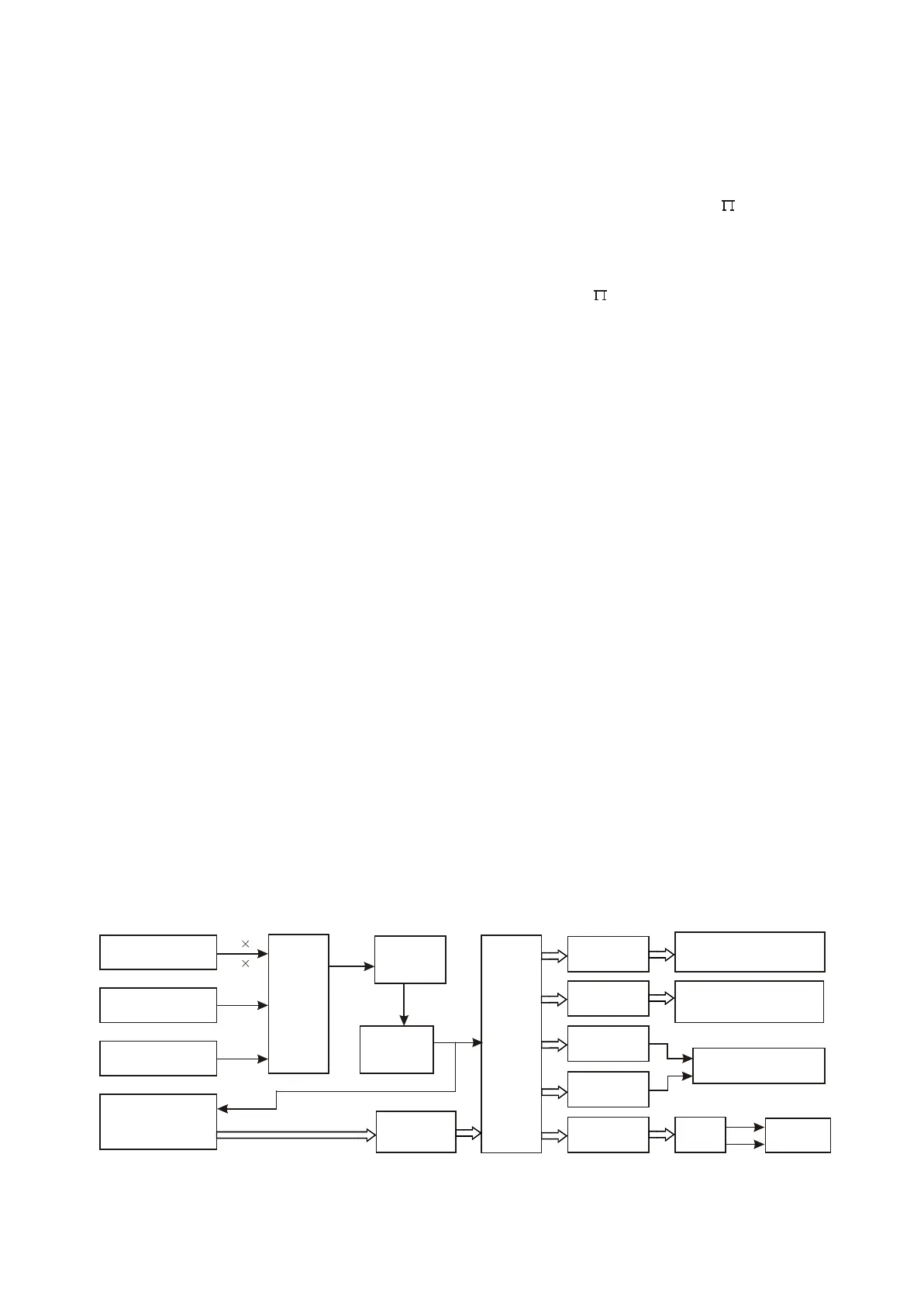
1. Audio power amplifying circuit block diagram is shown in the following figure 3.2.7.1:
External audio input
MIC signal input
External audio input
AU R
AU L
OK
TUL
TUR
N5
CD4052
AINR
N7
CS5340
SDA
N4
74HCT125
AINL
SDA AD
N12
TAS5508PAG
Decode board
74HCT125
N3
OK
SDATAO,ADATA1,ADATA2
Left channel LD
Right channel RO
TAS5112
N13
N14
TAS5112
N8
TLV272
N9
TLV272
N10
4580
Surround left/right channel,
subwoofer channel output
on power amplifier board
Front left/right channel,
centre channel output on
power amplifier board
AV board left/right
channel output
N11
4580
Headphone
output
H-R
H-L
Figure 3.2.7.1 Audio power amplifying circuit block diagram