3. Pin function is shown as the following table:
Pin Name Voltage in actual test Pin Name Voltage in actual test
1 DC/NC 0 5 SDA 3.21
2 RST _/NC 0 6 SCL 0
3 WP/RST 0 7 WP 0.29
4 VSS 0 8 VCC 3.21
Note: when playing DVD, CD disc and no disc in, the measured voltage are all the same, in which pin 7 is
protection-write pin, unused.
3.5.6 Function introduction to 74HCT125
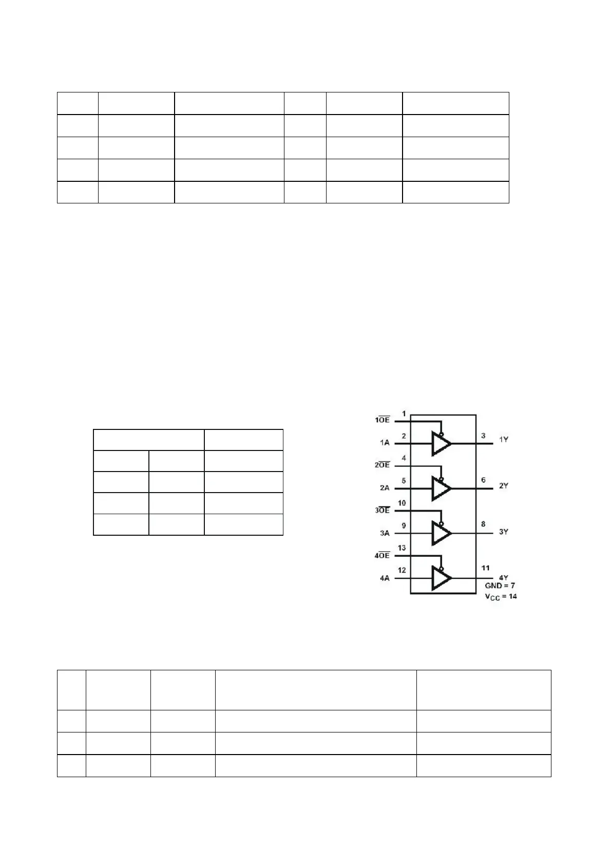
1. 74HCT125 (N3, N4) is a 4-channel gating switch, and each channel has its own gating signal, in which
pin 1, 4, 10 and 13 are gating control pins, gating when in low level and off when in high level. 74HCT125 truth
value table and function module structure is shown as the figure 3.5.6.1:
H: means high level (3.3V) L: means low level (0V)
X: means any state Z: means that is off and cannot
be selected
OUTPUTS
NA NOE NY
H L H
L L L
X H Z
INPUTS
Figure 3.5.6.1 Truth value table and 74HCT125 function module structure
2. Pin function of N3 (74HCT125) is shown as the following table:
Pin
Contiguous
signal name
Data direction
Function description
Directly contiguous element or
signal
1 M1 I Clock gating signal M1
2 MCLK I Clock signal input
Pin 4 of N2 (SN74LVC2G04DBVR)
3 MCLK O Clock signal output R70
- 81 -