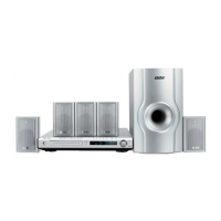
2. On the basis of 1389B, 1389E uses some pin functions again, and reduces USB function, so it
shows concise, video output pin is used again, the brightness signal, chroma signal, CVBS signal and
component video signal decoded through U201 (MT1389), through low pass filtering and clipping, are
sent to the corresponding terminal for output, shown in the figure 3.2.9.2:
HSYNC#
VSYNC#
R/Y
B/C
G
CVBS
B/C
R/Y
GND
VDATA3
IEC958
R223
75R
2
3
4
1
5
6
8
9
10
7
11
12
13
XS206
XS11
L376
FBSMT
L377
FBSMT
L378
FBSMT
L379
FBSMT
L380
FBSMT
L381
FBSMT
L382
FBSMT
L383
FBSMT
L384
FBSMT
L385
FBSMT
Video circuit diagramfigure 3.2.9.2
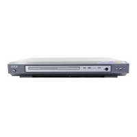
3. 3.2.9.3 This circuit is very simple, R106 is a matched resistor,
which makes signal achieve the max power on load; capacitorC106, C108 and inductor L106 compose a
low pass filter to filter high frequency interference signal except for useful signals; diode VD108, VD109
compose a limiting circuit; we know from features of diode that the max limitation of chroma signal Y
cannot be more than 5.7V, and the min cannot be less than -0.7V, thus the high voltage signals from TV
set can be prevented from burning down the player.
is shown in the following figure .
1
2
3
4
5
6
7
8
9
10
11
12
13
XP206
CON13
L
4
5
R
6
XC104B
AV4
L103
L
L104
L
L105
L
VIDEO_C
D+5V
R103
68R
SPDIF
Y1
Y2
Y3
Y4
Y5
Y6
R105
75R
C106
47P
C108
47P
L106
1.8uH
D+5V
Y1
R106
75R
C107
47P
C109
47P
L107
1.8uH
D+5V
Y2
R107
75R
C110
47P
C111
47P
L110
1.8uH
D+5V
Y3
R108
75R
C112
47P
C114
47P
L111
1.8uH
D+5V
Y4
R109
75R
C113
47P
C115
47P
L114
1.8uH
D+5V
Y5
R110
75R
C116
47P
C117
47P
L116
1.8uH
D+5V
Y6
VIDEO_Y
VIDEO_C
VIDIO
U
VIDIOV
VY
VV
VU
VDATA3
VSYNC
HSYNC
VIDI
O COMP
C105
224
L119
L
L118
L
L120
L
GND
1
VCC
2
OUT
3
XC106
TORX178A
1
2
3
4
5
6
7
XC105
DASW-02
L
1
2
R
3
XC104A
AV4
COAXIAL
VD100
1N4148
VD101
1N4148
VD102
1N4148
VD103
1N4148
VD104
1N4148
VD105
1N4148
VD106
1N4148
VD107
1N4148
VD108
1N4148
VD109
1N4148
VD110
1N4148
VD111
1N4148
C120
104
Green
Blue
Red
R129
220R
R130
100R
SPDIF
C121
20P
C122
20P
C123
20P
C124
20P
C125
20P
C126
20P
Y
Cr/Pr
Cb/Pb
VIDI
O COMP
VIDI
O
Video circuit diagramfigure 3.2.9.3
- 29 -