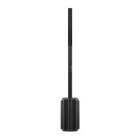
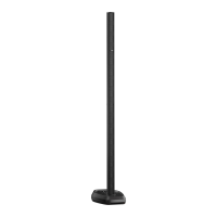
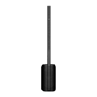
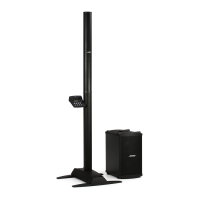
39
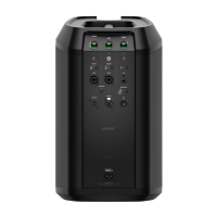
Disassembly Procedures
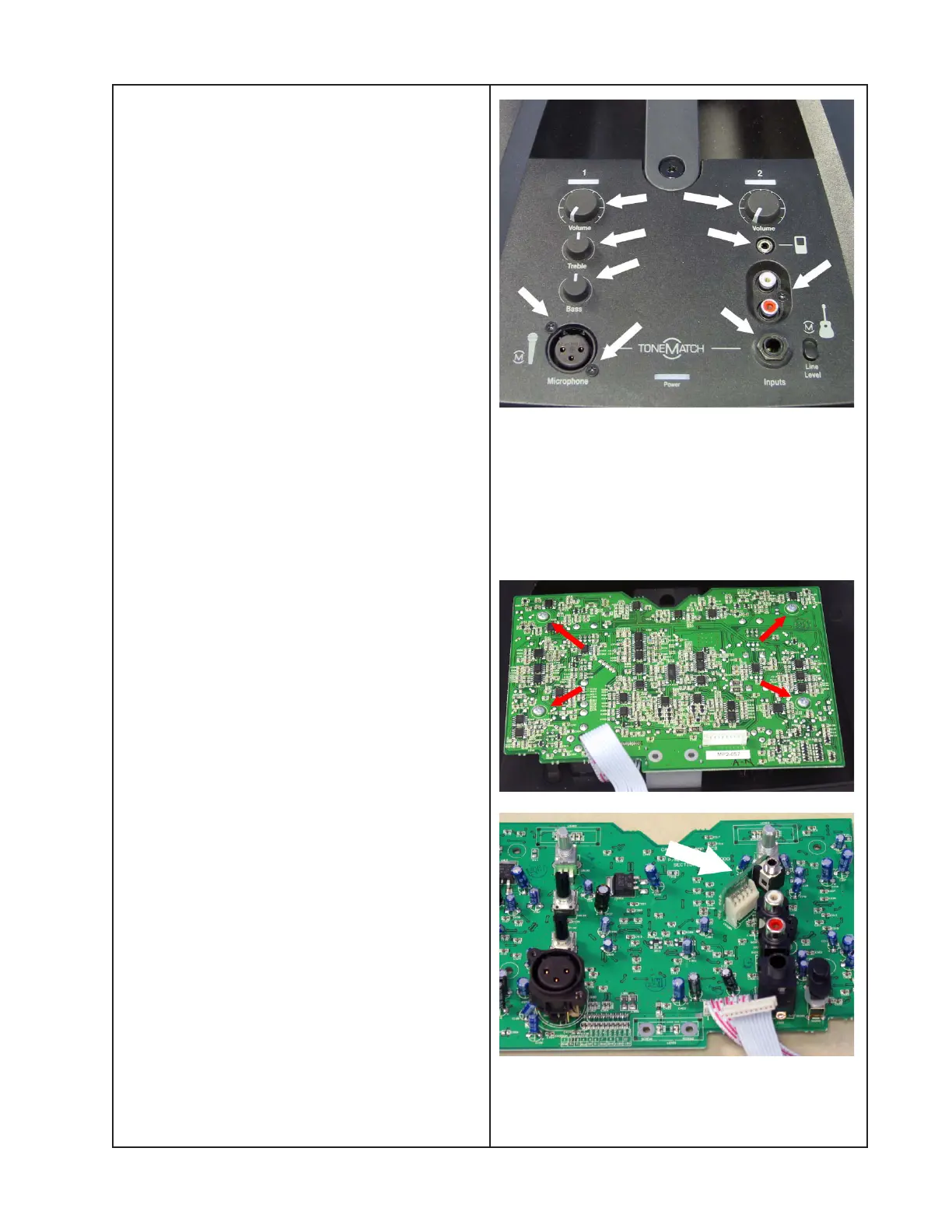
2. Input / Output PCB Removal
CAUTION: The SMD integrated circuits used
on the Input / Output PCB are extremely
sensitive to ESD damage. Be sure to use an
approved and tested ESD strap that is
properly grounded to your work bench before
attempting disassembly or repair of the L1
Compact Power Stand.
2.1 Perform procedure 1.
2.2 Remove the four knobs (volume 1,
volume 2, treble, bass) on the Input/Output
panel.
2.3 Remove the following items from the
top cover:
• two screws at the microphone jack.
• one screw at the RCA input jacks.
• ring at the 3.5mm input jack.
• hex nut at the 1/4” input jack.
2.4 Turn over the top cover. Remove the four
screws that secure the I/O board. Lift off the
board.
3. Jack Input PCB Removal
Note: The jack input PCB is a plug-in
daughter card located on the I/O PCB.
3.1 Perform procedure 2.
3.2 Unplug the jack input PCB from the I/O
PCB at connector CN308A. Lift off the board.
 Loading...