49
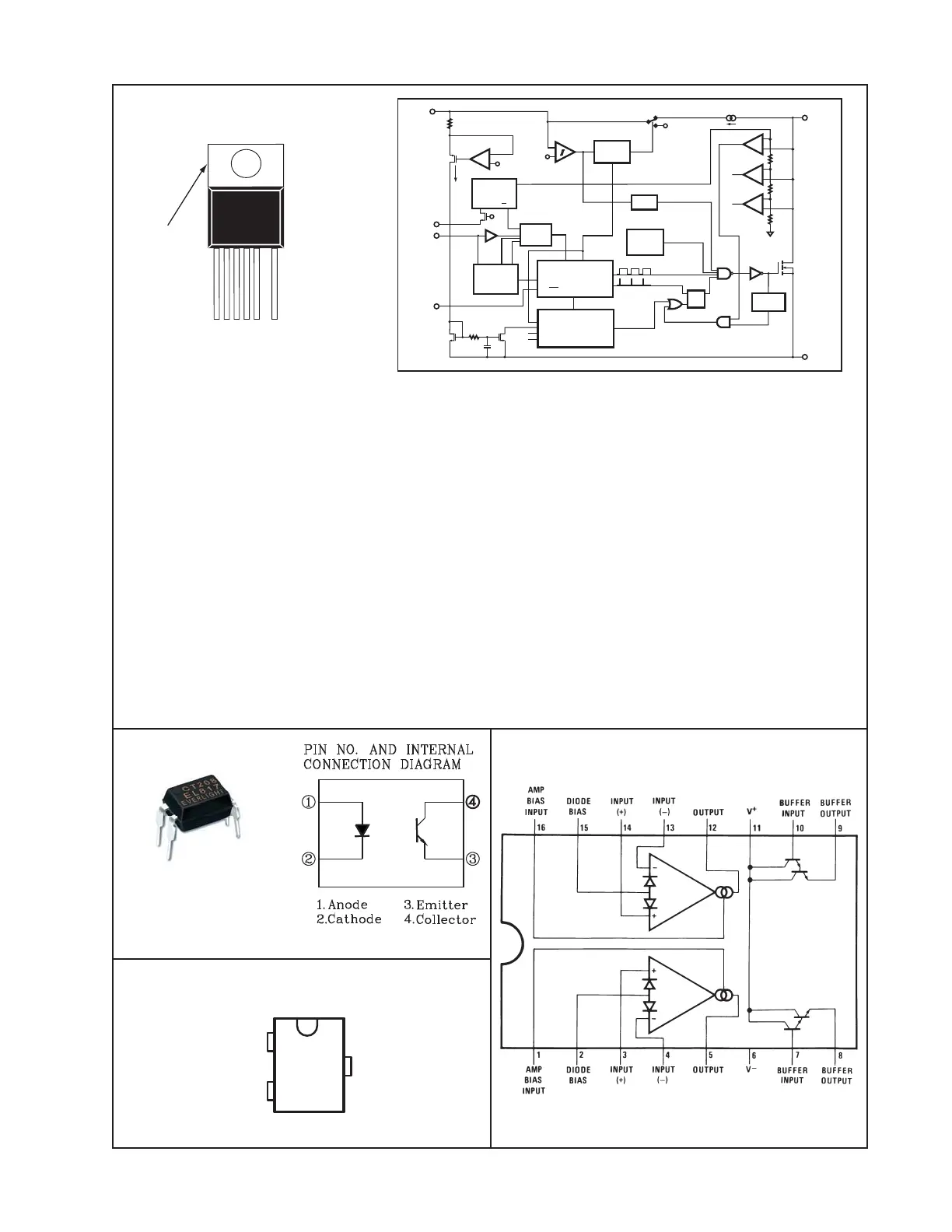
Functional Block Diagram (TOP254-258 YN Package)
PI-4511-082907
SHUTDOWN/
AUTO-RESTART
CLOCK
CONTROLLED
TURN-ON
GATE DRIVER
CURRENT LIMIT
COMPARATOR
INTERNAL UV
COMPARATOR
INTERNAL
SUPPLY
5.8 V
4.8 V
SOURCE (S)
SOURCE (S)
S
R
Q
D
MAX
STOP
SOFT
START
CONTROL (C)
VOLTAGE
MONITOR (V)
FREQUENCY
(F)
-
+
5.8 V
I
FB
1 V
Z
C
C
+
-
+
-
+
-
LEADING
EDGE
BLANKING
÷ 16
1
HYSTERETIC
THERMAL
SHUTDOWN
SHUNT REGULATOR/
ERROR AMPLIFIER
+
-
DRAIN (D)
ON/OFF
DC
MAX
DC
MAX
66k/132k
0
OV/
UV
OVP V
V
I (LIMIT)
CURRENT
LIMIT
ADJUST
V
BG
+ V
T
LINE
SENSE
SOFT START
OFF
F REDUCTION
F REDUCTION
STOP LOGIC
EXTERNAL
CURRENT
LIMIT (X)
OSCILLATOR
WITH JITTER
PWM
K
PS(UPPER)
K
PS(LOWER)
SOFT START
I
FB
I
PS(UPPER)
I
PS(LOWER)
K
PS(UPPER)
K
PS(LOWER)
Pin Con guration (Top View).
Tab Internally
Connected to
SOURCE Pin
Y Package (TO-220-7C)
7
D
5
F
4
S
3
C
2
X
1
V
Note: Y package for TOP254-258
Pin Functional Description
DRAIN (D) Pin:
High-voltage power MOSFET DRAIN pin. The internal start-up
bias current is drawn from this pin through a switched high-
voltage current source. Internal current limit sense point for
drain current.
CONTROL (C) Pin:
Error ampli er and feedback current input pin for duty cycle
control. Internal shunt regulator connection to provide internal
bias current during normal operation. It is also used as the
connection point for the supply bypass and auto-restart/
compensation capacitor.
EXTERNAL CURRENT LIMIT (X) Pin (Y, M, E and L package):
Input pin for external current limit adjustment and remote
ON/OFF. A connection to SOURCE pin disables all functions
on this pin.
VOLTAGE MONITOR (V) Pin (Y & M package only):
Input for OV, UV, line feed forward with DC
MAX
reduction, output
overvoltage protection (OVP), remote ON/OFF and device reset.
A connection to the SOURCE pin disables all functions on this pin.
FREQUENCY (F) Pin (TOP254-258Y, and all E and L packages):
Input pin for selecting switching frequency 132 kHz if connected
to SOURCE pin and 66 kHz if connected to CONTROL pin.
The switching frequency is internally set for xed 66 kHz
operation in the P, G, M package and TOP259YN, TOP260YN
and TOP261YN.
SIGNAL GROUND (G) Pin (TOP259YN, TOP260YN &
TOP261YN only):
Return for C pin capacitor and X pin resistor.
SOURCE (S) Pin:
Output MOSFET source connection for high voltage power
return. Primary side control circuit common and reference point.
IC Diagrams
TOP258YN PWM Controller
EL817
Connection Diagram
Top View
SOT23-3 PACKAGE
(TOP VIEW)
1
2
3
CATHODE
REF
ANODE
TL432BIDBZR Regulator LM13700 Transconductance Amplifier
EL817 Photocoupler
 Loading...