- 14 -
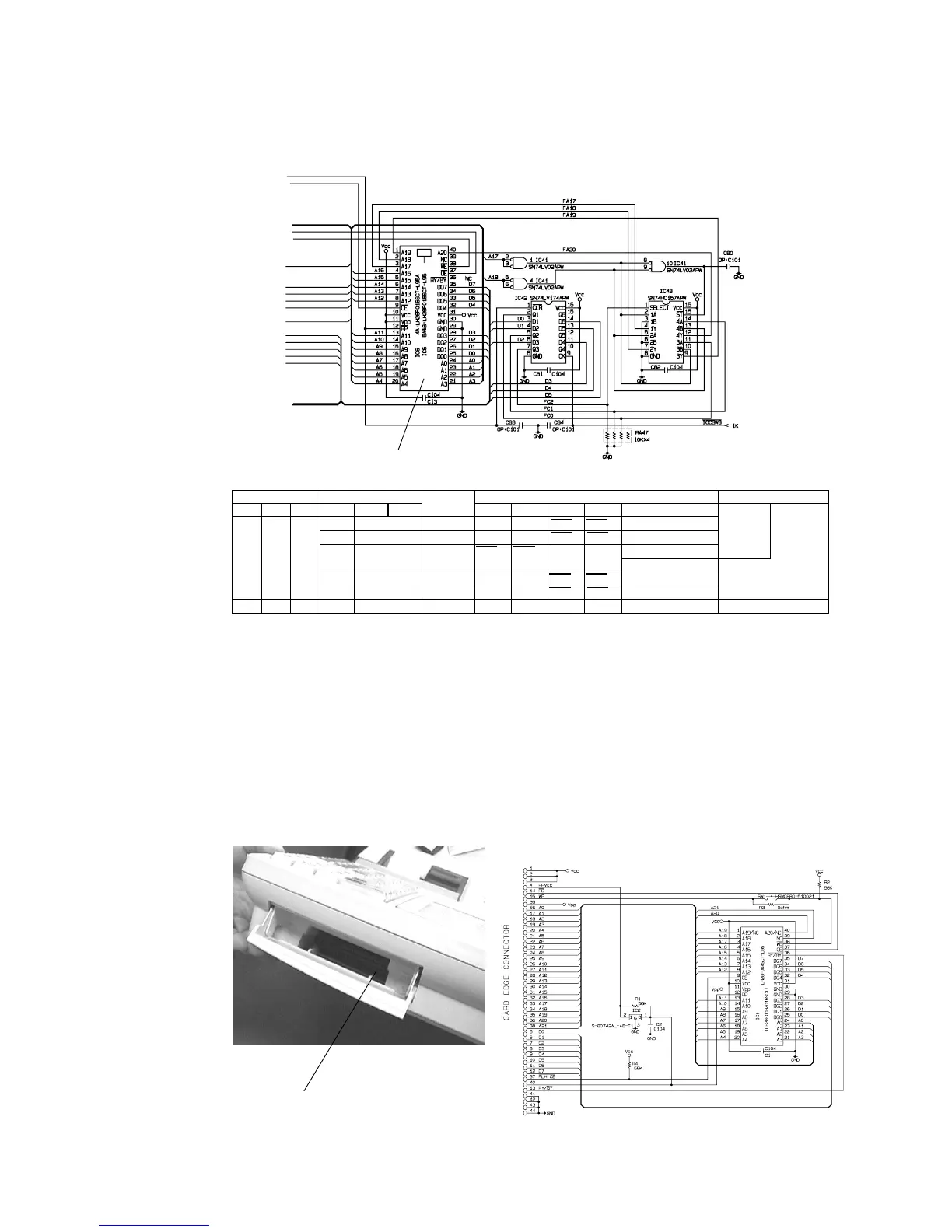
6-5. Flash ROM1 address circuit
The Flash ROM1 address signals FA17 to FA20 are made by the following circuit.
The Flash ROM1 (LH28F016SCT-L95, 16M bits) is used for the application program.
Flash ROM1 (16M bits)
CPU address BANK port Flash memory address NOTE
A19 A18 A17 FC2 FC1 FC0 BANK FA20 FA19 FA18 FA17 Memory block No. 8M bank 16M bank
H L L L L L 0 L L A18 A17 02 to 07
L H L L H 1 L H A18 A17 0A to 0F
H L H X X 2 A18 A17 L L 08,09
10,11,18,19
L H L 3 H L A18 A17 12 to 17
L H H 4 H H A18 A17 1A to 1F
H H H X X X Common LLLL00,01 Common
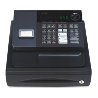
6-6. Flash Pack circuit (Memory Cassette RAC-9)
The Memory Cassette RAC-9 (2 M bytes) is possible to connect to the Flash Pack connector
CN17 of the Main PCB E475-1.
Flash Pack connector
[RAC-9 circuit diagram]