2-2. Operation of Control Parts
CLP-621 & CLP-631 2-34
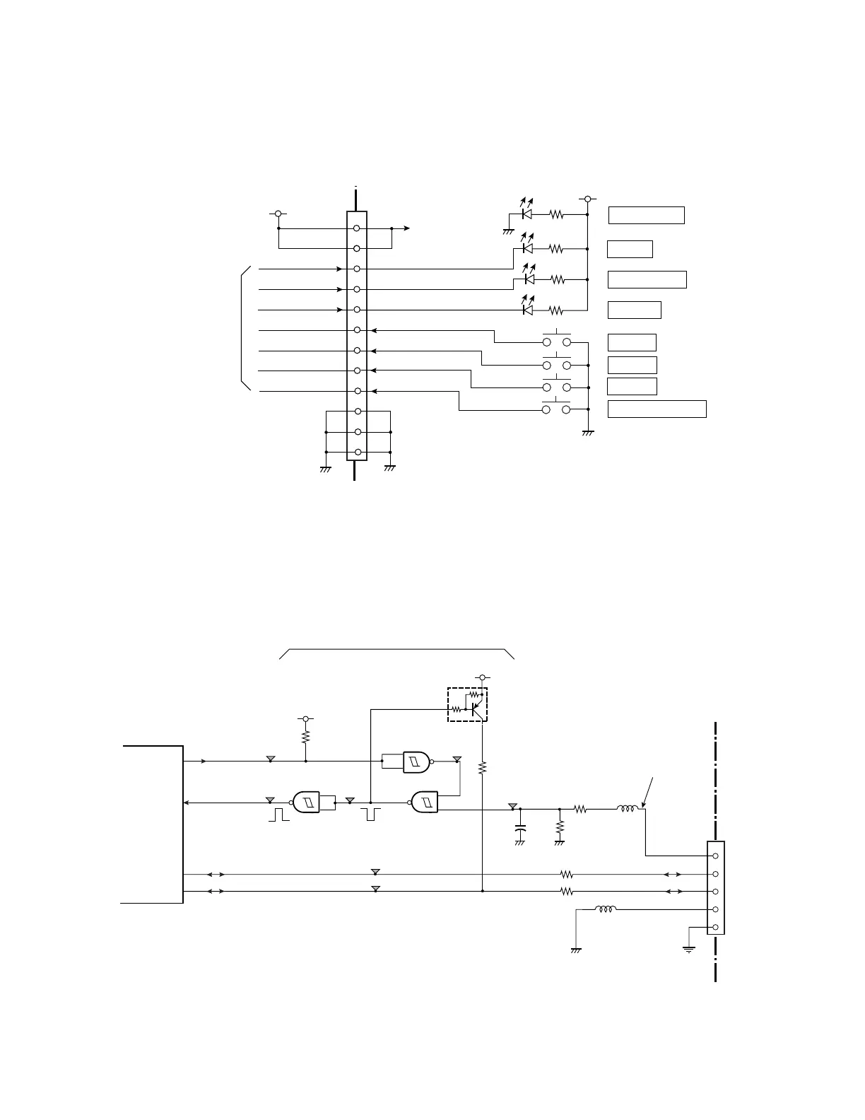
(5-4) Ope-pane circuit
The ope-pane circuit consists of 4 LEDs and 4 switches.
Each LED is directly driven by the Custom IC (IC11) and each switch signal is input to the
Custom IC (IC11). (The following shows the simplified circuit diagram.)
3
4
1
4
5
2
CN12
6
7
8
+3.3V
[Main PCB]
9
10
11
12
PRTLED
CNDLED
ERRLED
STOPSW
MODESW
PAUSESW
FEEDSW
+3.3V
[Ope-pane PCB]
POWER ON (Green)
PRINT (Green)
CONDITION (Orange)
ERROR (Red)
FEED
PAUSE
STOP
MODE/REPEAT
+3.3V
D304
D303
D302
SW302
SW303
SW304
SW301
D301
To/From
IC
11 Custom IC
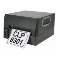
(5-5) USB I/F control circuit
The USB control circuit interfaces with the USB (Universal Serial Bus).
NAND gates (IC19) and transistor DTR5 consist of a USB connection detecting circuit.
When USB connector is connected, pin 1 of CN20 (USBVCC) is at “High” level. The
detection circuit detects this level and output a UBINTP pulse to the CPU.
1
2
3
4
5
P290
R151
P284
P286
R148
L2
P288
CN20
R150
P289
P287
R152
DTR5
DTA143EUA
C93
R149
UBINTP
UDP
UDM
SHIELD
USBVCC
USBLGND
DP
DM
USB I/F
L1
1
3
2
9
8
10
4
6
5
+3.3V
+3.3V
IC1
CPU
USBON
P11
155
D23
121
160
161
UDP
UDM
P285
[Main PCB]
High when USB
connector is connected.
USB connection detecting circuit
R147
IC19C
IC19B
IC19A