3-1
Technical description
Chapter 3: Technical description98-144591-D
Technical description
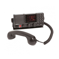
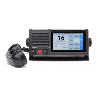
3.1 Control Unit
The Control Unit consists of a main module 60-127962 and two sub modules: HMI module 60-127963
and the Intercon module 60-127964.
The main module consists of the digital part, i.e. the microprocessor, program FLASH, SDRAM, TU-CU
Bus communication driver and Ethernet interface.
The main module also consists of an analog part, i.e. the voltage regulators, the analog interface circuits
and the analog output drivers (audio and light). The main module supports a build-in speaker and the
connectivity of an external 8 ohm speaker. The module also controls the the graphical TFT color display
(240x320 dots).
The HMI module contains a small keyboard interface and encoders for volume and rotary knob.
The Intercon module contains the connectors for external interfaces.
3.2 Transceiver Unit
The Transceiver Unit consists of four modules. Two modules located in the base part of the unit: a Sup-
ply Filter module, an Exciter Control module, and two modules are located in the door part of the unit:
a power amplifi er module including fi lter bank and a switched mode power supply. The main wiring is
by ribbon cables with Micro Match connectors. RF signals are routed in coaxial cables.
3.3 Supply Filter module 57-139985
To reduce electromagnetic interference even when transmitting at high power, a supply fi lter PCB consisting
of a common mode choke and high voltage decoupling capacitors is integrated in the transceiver unit.
There are no serviceable parts on this PCB.
3.4 Exciter Control module (ECM) 60-139984
The ECM board is the main board of the system 6000B MF/HF. This board consists of the following
main items:
• Local power supplies generating supplies to the integrated circuitry present on the ECM board.
• RF input with Surge Arrester (90VDC +/-20% and in accordance with ITU-T Rec. K.12 and
DIN 57845/VDE0845) .
• Anti-aliasing and power line noise fi lter with pass band of 150kHz to 30MHz.
• Variable Gain Amplifi er and input overload protection.
• 16 bit Analog to Digital Converter sampled at 98.304MHz generated by 0.3ppm local oscillator
on 17.8176MHz
• FPGA doing direct sampling, multiple receiver chains, fi ltering, SWR protection and direct
up-conversion transmitter chain.
• Flash ADC used as input to protection circuitry yielding response time in microseconds towards
bad SWR.
• Dual TX DAC modulating directly on the transmitter frequency.
• Broad band high linearity amplifi er outputting RF signal at approximately +9 dBm.
• DSP for signal processing, modulation schemes, power loop, modem and ATU control.
• FSK modem for communication with the antenna tuning unit.
• ARM processor with DDR3 RAM and eMMC Flash for LAN connectivity, control and boot of
other peripherals. Furthermore, NMEA, real time clock and CAN.
Chapter 3

 Loading...