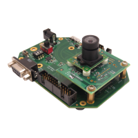
Cypress EZ-USB CX3
EZ-USB® CX3 Technical Reference Manual, Doc. No. 001-91492 Rev. *B 33
1.13 Glossary
Application Programming Interface. A series of software routines that comprise an
interface between an application and lower-level services and functions (for example
interfaces to configure and control the FX3/CX3 device operation).
The EZ-USB FX3 SDK provides a set of libraries which provide APIs to configure and
control the operation of the FX3 device.
A color filter array for arranging RGB color filters on a square grid of photo sensors. The
filter pattern is 50% green, 25% red and 25% blue.
The EZ-USB FX3/CX3 devices have an embedded 32-bit ARM926EJ-S core which
delivers processing capability of 200 MIPS. This ARM core is coupled with Instruction and
Data Caches, Tightly Coupled Memories (TCM), and a PL192 Vectored Interrupt
Controller (VIC). More details can be found in the FX3 CPU Subsystem chapter of the EZ-
USB FX3 TRM.
Unidirectional MIPI CSI-2 differential serial interface used for data transfer. Each lane
comprises two signals: Data+ and Data-. CX3 supports up to four Data lanes, each
capable of speeds up to 1 Gigabits per second.
The Direct Memory Access (DMA) subsystem performs high-bandwidth data transfers
between memories and peripherals without CPU intervention. The FX3/CX3 architecture
includes a DMA fabric that is used to steer data between various peripheral interfaces and
system memory. Details regarding the DMA subsystem can be found in the FX3 DMA
Subsystem chapter of the EZ-USB FX3 TRM.
FX3/CX3’s Global Controller (GCTL) unit contains a Clock Generation Block, Multifunction
I/Os, a Power Control Block, and a Reset Block. The Clock Generation block provides
clocks to all device peripherals. More details can be found in the FX3 Global Controller
(GCTL) chapter of the EZ-USB FX3 TRM.
The CX3 GPIF II interface is a fixed-function implementation of the General
Programmable Interface available in the FX3. The CX3 GPIF II interface is used to
transfer data from the MIPI CSI-2 receiver block. Details of the fixed-function GPIF II state
machine on the CX3 are available in Section 1.9 of this TRM supplement. More details
can be found in the General Programmable Interface II (GPIF II) chapter of the EZ-USB
FX3 TRM.
The I
2
C-bus protocol, created by Philips Semiconductor, stands for ‘Inter-Integrated Circuit
bus’ and allows data communication between I
2
C capable devices using two wires. It
sends information serially using a data (SDA) line and a clock (SCL) signal. FX3/CX3 can
function as a master I
2
C controller supporting 100 kHz, 400 kHz, and 1 MHz operation.
More details can be found in the I
2
C Interface section of the Low Bandwidth Peripherals
chapter of the EZ-USB FX3 TRM.
Joint Test Action Group (JTAG) is the common name for the IEEE 1149.1 Standard Test
Access Port and Boundary-Scan Architecture. FX3/CX3’s JTAG interface has a standard
5-pin interface to connect to a JTAG debugger to debug firmware using the on-chip debug
circuitry. Industry-standard debugging tools for the ARM926EJ-S core can be used for
debugging the FX3/CX3 devices.
Low-Bandwidth
Peripherals
FX3/CX3’s serial peripherals I
2
C, SPI, I
2
S and UART including GPIO form the Low-
Bandwidth Peripherals (LBP). More details can be found in the Low-Bandwidth
Peripherals chapter of the EZ-USB FX3 TRM.
The MCLK is an optional clock output from the CX3, which can be used as the input
reference clock for the image sensor. More details are available in Section 1.7.5 of this
TRM supplement.
The CX3 memory subsystem comprises system RAM that serves as program and data
memory, SRAM controller, and an Advanced High-performance Bus (AHB)-based
interconnect that allows the ARM CPU and the hardware blocks to access these
memories. The Memory Mapped I/O (MMIO) interconnect provides access to registers in
various peripheral blocks. More details can be found in the Memory and System
Interconnect chapter of the EZ-USB FX3 TRM.
Mobile Industry Processor Interface (MIPI) Alliance Standard for Camera Serial Interface 2
(CSI-2) is a serial camera interface defined by the MIPI Alliance. It defines standard data
transmission and control interfaces between the camera transmitter and receiver. The
data transmission interface is a unidirectional differential serial interface with data and
clock signals. More details on the MIPI CSI-2 specification can be obtained from the MIPI
Alliance website http://www.mipi.org/specifications/camera-interface

 Loading...