Cypress EZ-USB CX3
EZ-USB® CX3 Technical Reference Manual, Doc. No. 001-91492 Rev. *B 15
1.10 MIPI CSI-2 Block Registers
The MIPI CSI-2 block exposes a set of registers used to configure the block over I
2
C. The block is available
at the 7-bit I
2
C slave address 7'b0000111 (Read address 0x0F; Write address 0x0E). The block supports 100
kHz and 400 kHz I
2
C operation.
Note: No other I
2
C device with the same address as the MIPI CSI-2 block should be connected to the I
2
C bus
of the CX3 device.
The registers are 16-bit aligned, and data transfers are performed Most Significant Bit (MSB) first.
Figure 8 and Figure 9 show typical I
2
C Read and Write transfers to the MIPI CSI-2 block.
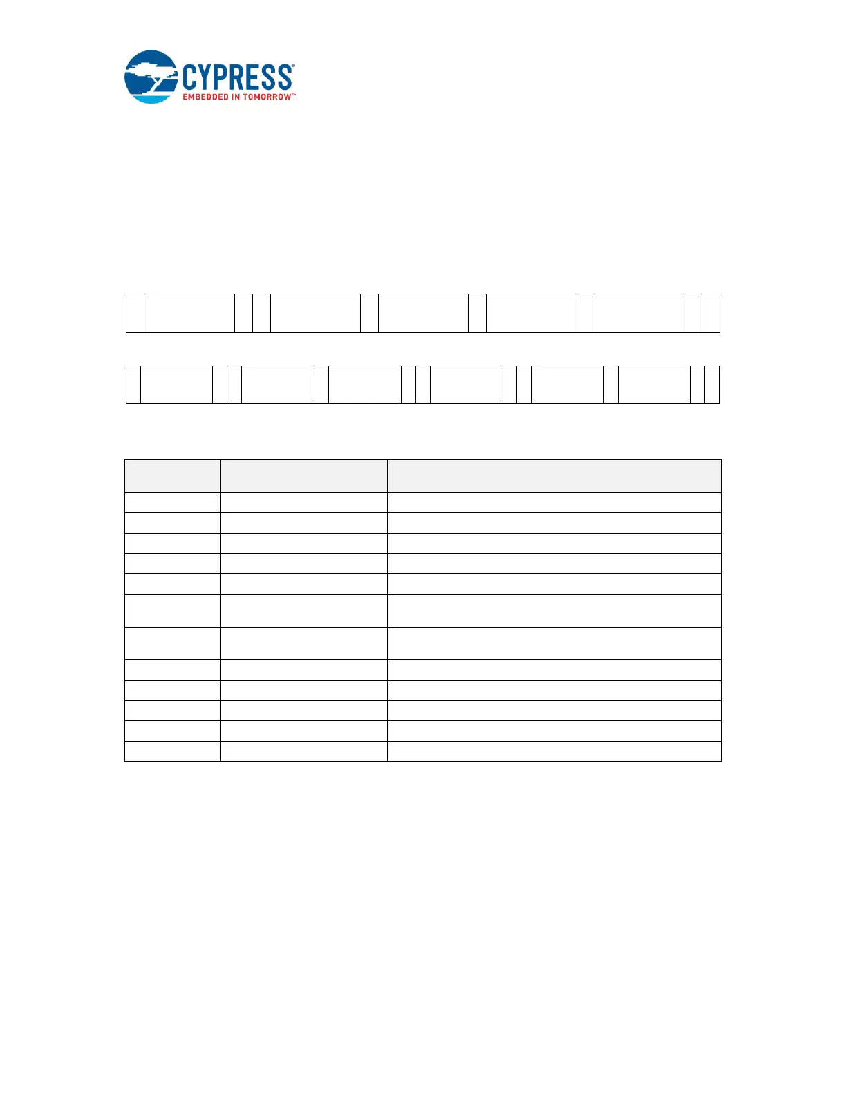
Figure 8. Write Transfer Sequence
S
SLAVE ADDRESS
7 bit (0000_111)
0 A
REG_ADDR_VAL
[15:8]
A
REG_ADDR_VAL
[7:0]
A DATA[15:8] A DATA[7:0] A P
Figure 9. Read Transfer Sequence
Table 5 provides a list of the configuration registers included in the CX3 MIPI CSI-2 block.
Table 5: MIPI CSI-2 Block Configuration Registers
Configuration Control Register
Data Format Control Register
Register to Enable MIPI CSI-2 signals (XRESET and
XSHUTDOWN)
Register to Control MIPI CSI-2 signals (XRESET and
XSHUTDOWN)
PLL Clock Control Register 0
PLL Clock Control Register 1
Register to set MIPI THS-Settle timer settings.
The following sections provide detailed descriptions of each of the CX3 MIPI CSI-2 configuration registers.
Note: RESERVED Register Bits should not be changed. When writing to a register with RESERVED bits, you
should ensure that the values are not changed during a Write (preferably by doing a Read before the Write
and maintaining the values for the RESERVED bits during the Write).
S
SLAVE ADDRESS
7 bit (0000_111)
1 A DATA[15:8] A DATA[7:0] A PS
SLAVE ADDRESS
7 bit (0000_111)
0 A
REG_ADDR_VAL
[15:8]
A
REG_ADDR_VAL
[7:0]
A
 Loading...


