Cypress EZ-USB CX3
EZ-USB® CX3 Technical Reference Manual, Doc. No. 001-91492 Rev. *B 11
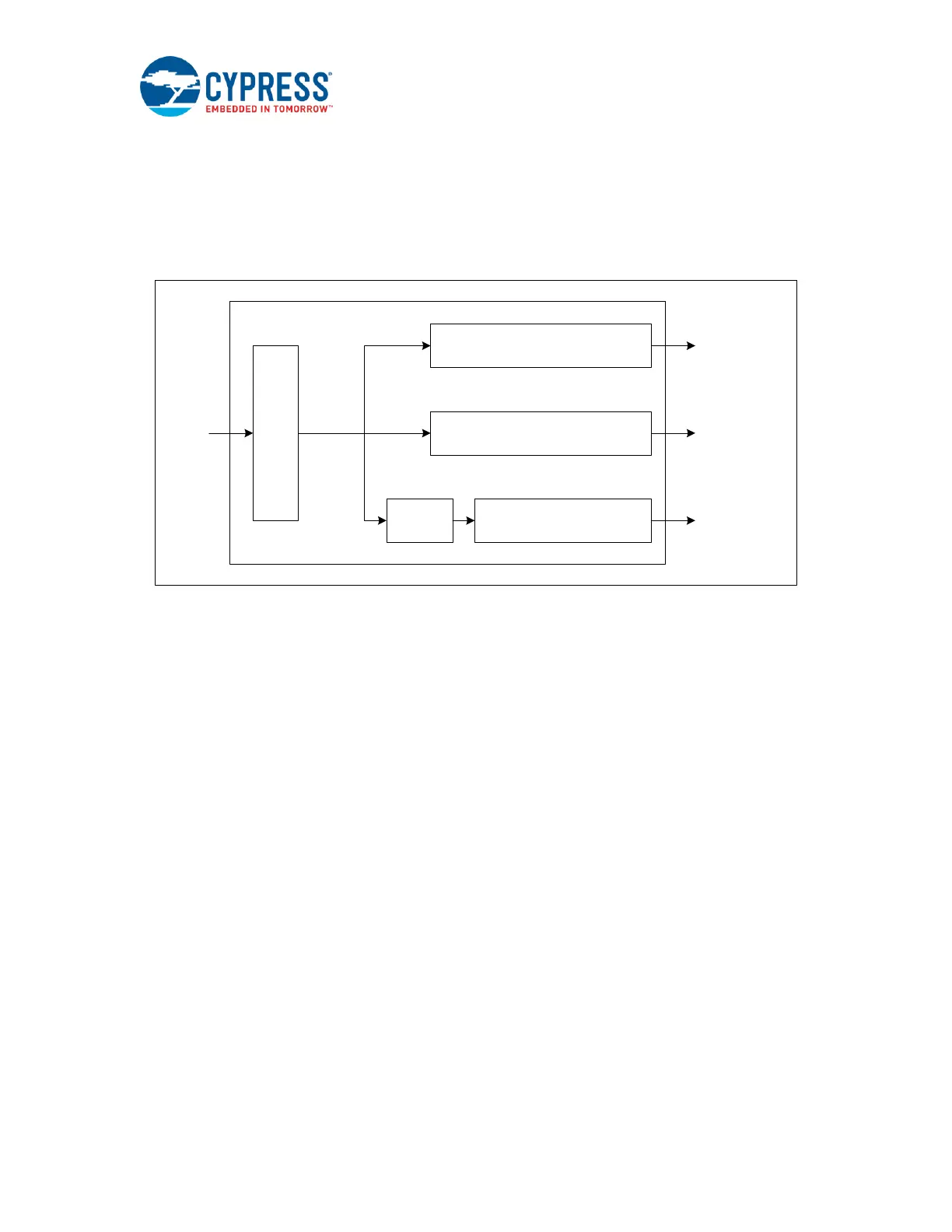
1.7 MIPI CSI-2 Block Clocks
Figure 6 shows the CX3 clocks on the MIPI CSI-2 block. The interface takes a reference clock as its input and
generates the required clocking using a PLL followed by multiple clock dividers. In the CX3 application
firmware, clock configuration parameters are a part of the CyU3PMipicsiCfg_t structure, which is passed to
the CyU3PMipicsiSetIntfParams() API to configure the CSI-2 block. Details of the structure and configuration
API can be found in the EZ-USB FX3 SDK Firmware API Guide.
Figure 6. CX3 MIPI CSI-2 Block Clocks
A brief description of each of the clocks is provided in the following sections.
1.7.1 Reference Clock (REFCLK)
This is the reference clock input provided to the MIPI CSI-2 block. This input clock should be between 6 and
40 MHz.
1.7.2 PLL Clock (PLL_CLK)
The PLL_CLK is the primary clock of the MIPI CSI-2 block. The value for PLL clock should be between
62.5 MHz and 1 GHz. All other internal and output clocks are derived from this clock.
The PLL clock frequency is generated from the input reference clock using the following equation:
PLL_CLK = REFCLK * [(PLL_FBD + 1) / (PLL_PRD + 1) ] / (2^ PLL_FRS)
Where
PLL_FBD is the feedback divider whose range is between 0 and 0x1FF.
PLL_PRD is the input divider whose range is between 0 and 0x0F.
PLL_FRS is the frequency range selection parameter that takes the following values:
‘0’ if the PLL clock is between 500 MHz and 1 GHz.
‘1’ if the PLL clock is between 250 MHz and 500 MHz.
‘2’ if the PLL clock is between 125 MHz and 250 MHz.
‘3’ if the PLL clock is between 62.5 MHz and 125 MHz.
Sample computations for the PLL clock frequency are provided for a REFCLK value of 19.2 MHz in the
following table:

 Loading...


