EPSON Stylus C50/C60/C61/C62 Revision C
Operating Principles Electrical Circuit Operating Principles 42
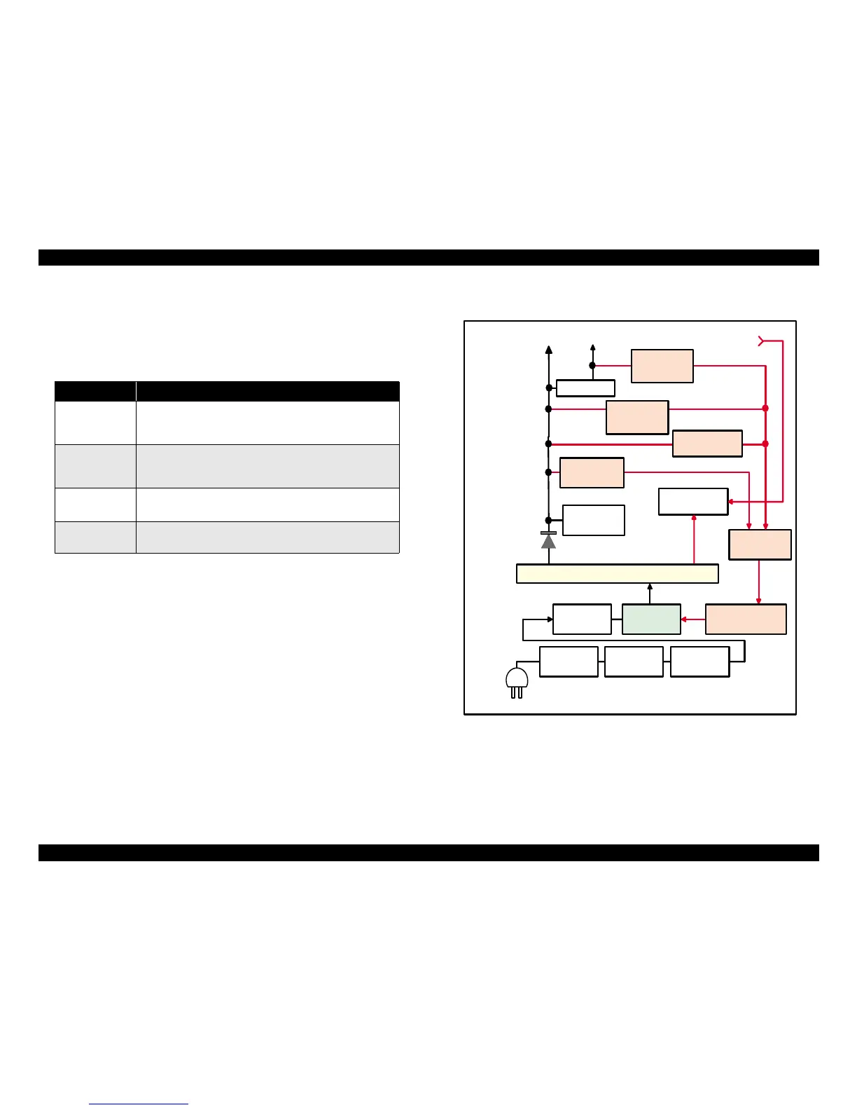
2.2.1 C417 PSB/PSE board, C482 PSH board
The power supply boards of the Stylus C50/60/C61/C62 use a RCC (Ringing Chalk
Converter) circuit, which generates +42VDC for drive line and +5VDC for logic line to
drive the printer. The application of the output voltage is described below.
Table 2-6. Application of the DC Voltages
AC voltage input from AC inlet first goes through filter circuit that removes high
frequency components and is then converted to DC voltage via the rectifier circuit and
the smoothing circuit. DC voltage is then lead to the switching circuit and FET Q1
preforms the switching operation. By the switching operation of the primary circuit,
+42VDC is generated and stabilized at the secondary circuit. This +42VDC generated
by the secondary circuit is converted to +5VDC by the chopping regulator IC of the
secondary circuit.
2.2.1.1 C417 PSB/PSE board
Figure 2-18. C417 PSB/PSE board block diagram (Stylus C50/C60)
The C417 PSB/PSE board has the various control circuits to stop voltage output if a
malfunction occurs on the power supply board or the main board while the printer
mechanism is on duty. Following explains each control and protection circuit.
Voltage Application
+36VDC
(Stylus C50)
• Motors (CR Motor, PF Motor)
• Printhead common voltage
• Printhead nozzle selector 42V drive voltage
+42VDC
(Stylus C60/C61/
C62)
• Motors (CR Motor, PF Motor)
• Printhead common voltage
• Printhead nozzle selector 42V drive voltage
+5VDC
(Stylus C50/C60)
• C418/C429/C483/C484 Main control circuit logic
•Sensor/LED
+3.3VDC
(Stylus C50/C60)
• C483/C484 Main control circuit logic
•Sensor/LED
+5VDC Line
Over Voltage
Limitation
+42VDC Line
Over Voltage
Limitation
+42VDC Line
Drop Limitation
+42VDC Line
Constant
Control
Smoothing
Circuit
+5V Regulator
Power Drop
Delay Circuit
Photo Coupler
TRANS(T1)
PSC Signal
from Main board
ZD53
+5VDC+42VDC
IC51
R91,R92,R93,Q91,ZD51
ZD52,87
ZD90
C84,Q84
C51
Q1C11
D51
Q2,Q3,Q31
Abnormally Feed
back circuit
Main
Switching
Circuit
Smoothing
Circuit
Over Current
Protection
Filter Circuit
Full Wave
Rectifier circuit
DB1
L1,C1
F1,TH1
AC Input
PC1