n
Adjustment
–
Connect the probe tip to the center hole of J7.The sur
-
rounding holes are suitable ground connections. See Fig
-
ure 7-2.
–
Adjust R196 until the pulses on the oscilloscope look
the same. See Figure 7-3. Use a screwdriver type of ad
-
justment tool.
–
Check Step Response X1, repeat Step Response X1 and
Linearity several times if necessary.
Repeat all steps above for Input B on the tim er/counter. Con
-
nect the probe tip to J9. Adjust R268.
Sensitivity
n
Setup
–
Keep the settings on the counter from Linearity.
n
Adjustment
–
Connect the DMM to the test points X34 (+) and X35
(-). See Figure 7-2.
–
Adjust R197 until the DMM reads +17 ± 0.2 mV. Use a
screwdriver type of adjustment tool.
Don't forget to resolder the RF shield.
Power Supply
n
Setup
–
Do as described under Preparations above.
–
Select default settings by keying in
USER OPT ®
Save/Recall ® Recall Setup ® Default
n
Adjustment
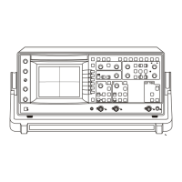
–
Connect the DMM to test point X9 and ground (metal
shield lid over input amplifiers). See Figure 6-4 and
Figure 7-4.
–
Adjust the +5 V trimmer on the AC/DC power supply
board with a screwdriver type of adjustment tool until
the DMM reads +5.10 ± 0.005 V.
–
Check that the voltage from the AC/DC power supply at
X26 is +15 ± 0.7 V.
–
Check that the voltage from the AC/DC power supply at
X21 is -15 ± 0.7 V.
Note: Adjusting the +5 V does not affect other settings in the
instrument.
External Reference Input
n
Setup
–
Do as described under Preparations above.
–
Select default settings by keying in
USER OPT ®
Save/Recall ® Recall Setup ® Default
–
Connect a 1 MHz sinewave signal with amplitude 0.1
V
rms
(0.28 V
pp
) into 50 W from an LF synthesizer to the
external reference input. Use a 50 W termination on the
input.
– Set an oscilloscope with X10 probe to 10 ms/div,
100 mV/div (including probe) and AC coupling.
n
Adjustment
– Connect the probe to X19. There are two ground pads in
the vicinity. See Figure 7-5.
– Adjust C442 to maximum amplitude. Use a screwdriver
type of adjustment tool.
Power Supply 7-13
+5 V adj.
J17
X26
X9
X21
GND
AC/DC BOARD
RF SHIELD
Figure 7-4 Adjusting +5 V and checking +15 V and -15 V.
C442
X19
GND
GND
AC/DC BOARD
J22
J25
J23
J26
J21
Figure 7-5 Adjusting the external reference input.