Contents
C156-E228-02EN xiii
Illustrations
FIGURES
Figure 1.1 The optical disk drive (with panel)............................................. 1-6
Figure 1.2 The optical disk drive (without panel)........................................ 1-6
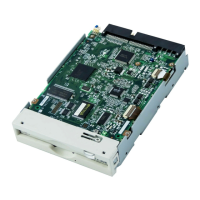
Figure 1.3 Configuration of optical disk drive.............................................1-7
Figure 1.4 Block diagram of the control circuit section...............................1-9
Figure 2.1 Optical disk cartridge .................................................................2-8
Figure 2.2 Algorithms for alternate processing.......................................... 2-11
Figure 2.3 Example of alternate processing............................................... 2-12
Figure 3.1 Surface temperature measurement point ...................................3-1
Figure 3.2 Outer dimensions .......................................................................3-5
Figure 3.3 Outer dimensions .......................................................................3-7
Figure 3.4 Installation directions................................................................3-10
Figure 3.5 Center of gravity .......................................................................3-11
Figure 3.6 Mounting frame structure .........................................................3-12
Figure 3.7 Service areas .............................................................................3-13
Figure 3.8 MCM3130SS current waveform (+5 VDC) .............................3-14
Figure 3.9 Power on/off sequence (1) ........................................................3-15
Figure 3.10 Power on/off sequence (2) ........................................................3-15
Figure 3.11 Power on/off sequence (3) ........................................................3-15
Figure 3.12 AC noise filter (recommended) ................................................3-16
Figure 3.13 Connector and terminal locations .............................................3-17
Figure 3.14 Power supply connector............................................................3-18
Figure 3.15 Cable connection mode.............................................................3-19
Figure 3.16 External operator panel circuit example...................................3-21
Figure 3.17 External operator panel interface connector.............................3-22
Figure 4.1 Individual packaging style..........................................................4-3
Figure 4.2 Gathered packaging style............................................................4-3
Figure 4.3 SCSI bus connection modes .......................................................4-4
Figure 4.4 Positions of setting terminals and switches ................................4-6
Figure 4.5 Setting switch (SW1)..................................................................4-7
Figure 4.6 SCSI connection check .............................................................4-16
Figure 5.1 Optical disk drive front view (with panel)..................................5-1