When the FORA/FORB voltage increased, the output from
the difference
amplifier will
be
decrease
to
reduce the IF
amplifier
gain. This adjusts the
RF
output power until the
FORA/FORB
and
POCO
voltages are well-balanced.
4-2-8 APC CIRCUIT
(PA-A, PA-B AND MAIN UNITS)
The
APC
(Automatic Power Control) circuit protects the
power
amplifiers
on
the PA-A
and
PA-B units from exces-
sive current.
Current drain of power
amplifiers
is
detected
by
voltage
drops
at
resistors (PA-A unit
R1,
R12
and
PA-B
unit
R1,
R16). The original voltage (IC1)
and
dropped voltage (AIC2
or
BIC2) are applied
to
the
APC
difference amplifier (MAIN
unit, IC4a or IC4b).
The signal output from the difference amplifier reduces IF
amplifier gain until these voltages are well-balanced.
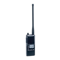
4-3 PLL CIRCUITS
IC-821
H contains 2 PLL circuits
and
1 local oscillator. The
VHF
and
UHF PLL circuits adopt
"I
com's original I-loop
PLL" to obtain very fast lock
up
times .
• PLL circuits
ICl
IC2a
4-3-1
VHF PLL CIRCUIT (PLL UNIT)
The VHF PLL circuit generates the 1
st
LO
frequency,
and
the signals are applied
to
the 1 st mixer circuits
in
the RF-A
unit. The
PLL circuit consists of a VCO, prescaler
and
DDS
circuits.
The
signal generated
at
the VHF
VCO
circuit (01, D1-D3,
D8)
is
amplified at the buffer-amplifiers (02, IC5), then
applied to the prescaler circuit (IC4). The prescaler circuit
divides the
applied signal, and outputs it to the VHF
DDS
circuit (lC1) via the buffer-amplifier (04). The VHF
DDS
circuit generates digital signals using the applied signal
as
a
clock frequency. The phase detector section
in
ICl
com-
pares it's phase with the reference frequency which
is
generated at the reference oscillator (Xl).
IC1
outputs
off-phase components
as
pulse signals via pins
52, 53.
The output pulses are converted into
DC
voltage
at
the loop
filter circuit (IC2a)
and
then applied
to
the VHF VCO circuit.
The D/A converter (R15-R38),
low-pass filter (L2-L4,
C4-C10)
and
buffer-amplifier (IC14) circuits are connected
to the
DDS
output to convert the digital oscillated signals
into smooth analog signals.
The output
DC
voltage from the loop filter circuit
is
also
applied
to the RF-A unit to control the tuned bandpass filter.
IC2b
>---
To RF-A board
01,01-03,08
I--_-_l,r-~
..
~··~,'l-------A-l-L-O-
To VHF 1 st mixer circuit
T
\..:l}
(RF-A board, 011,
012)
Xl: 30.2 MHz
L...-_--'
'
•.....•.......
_;
Prescaler
I---C
1/8
IC4
IC5 VHF PLL
circuit
r---------------------------
_________________________
..J
IC7b UHF PLL
circuit
-:>--_
To RF·B board
IC6
IC7a
05,04,010
I----+---:--~I
Phase
.--'---
__
1 detector
1-'---1
Loop
filter
1----4
__
i:r-~
..
~
..
~;:'
___
--..~B:....l~L:....O_
To UHF 1 st mixer circuit
T
\..:l}
(RF-B board, 014,
015)
'------'
' ..............
_;
Prescaler
I---C
1/8
08
IC9
09
014
B2LO T UHF
d'
..
1-----------
________
0
2n
mixer
CircUit
(RF-B board,
011)
>----------
To
BFO
circuits (MAIN unit,
ICl
01,
IC103)
024
4-6