SECTION 4 CIRCUIT DESCRIPTION
4-1
RECEIVER CIRCUIT
Note: [Main]=Main band, [Sub]=Sub
band
4-1-1 VHF ANTENNA SWITCHING CIRCUIT
(PA-A UNIT)
Received signals from the antenna connector
(J2)
are
passed through the low-pass filter (L3-L5,
C5-C8) then
applied
to
the antenna switching circuit
{01-03,
L6.
L7}.
The antenna switching circuit functions as a low-pass filter
while receiving. However, its impedance becomes very
high while transmitting by turning
ON
diodes (02, 03).
Thus transmit signals are blocked from entering the receiver
circuits.
The passed signals are then
applied to the RF-A unit.
4-1-2 VHF RF CIRCUIT (RF-A UNIT)
Received signals from the PA-A unit via J6 are applied
to
the
RF
amplifier circuit
(Q7)
via the
RF
attenuator (015)
and
tunable bandpass filter (013. L 16) circuits.
The amplified signals are then passed through the another
tunable bandpass
filter circuit (010-012, L
13-L
15) to sup-
press unwanted signals. The filtered signals are then
applied
to
the 1 st mixer circuit
(Qll
, Q12).
Varactor diodes
(010-013) are used for the bandpass
filters
to
tune the center frequency for wide bandwidth
receiving
and
good
image response rejection. PLL lock
voltages are applied
to
these diodes for tuning.
4-1-3 VHF 1ST MIXER CIRCUIT (RF-A UNIT)
The 1 st mixer circuit converts the received signals to a fixed
frequency of the
10
MHz
IF signal with a PLL output fre-
quency.
By
changing the
PLL
frequency, only the desired
frequency
will
be
passed through a pair of crystal filters at
the next stage of the VHF 1 st mixer .
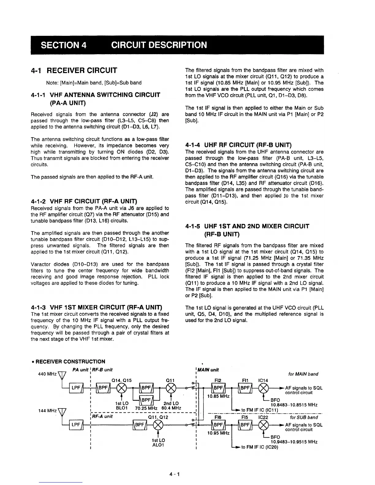
• RECEIVER CONSTRUCTION
440 MHz
PA unit: RF·B unit
014.015
4
-1
The filtered signals from the bandpass filter are mixed with
1 st
LO
signals at the mixer circuit
(Ql1,
Q12) to produce a
1st
IF signal (10.85
MHz
[Main] or 10.95
MHz
[Sub]). The
1
st
LO
signals are the PLL output frequency which comes
from the VHF
veo
circuit (PLL unit.
Q1.
01-03,
08).
The 1 st IF signal is then applied to either the Main or Sub
band
10
MHz
IF circuit
in
the
MAIN
unit via
P1
[Main] or
P2
{Sub].
4-1-4 UHF
RF
CIRCUIT (RF-B UNIT)
The received signals from the UHF antenna connector are
passed through the low-pass tilter
(PA-B unit, L3-L5,
C5-C10)
and
then the antenna switching circuit (PA-B unit,
01-03).
The signals from the antenna switching circuit are
then applied
to
the
RF
amplifier circuit (Q16) via the tunable
bandpass filter
(014,
L35)
and
RF
attenuator circuit {016}.
The amplified signals are passed through the tunable band-
pass filter
(011-013),
and
then applied
~o
the 1
st
mixer
circuit
(Q14,
Q15).
4-1-5 UHF 1ST AND 2ND MIXER CIRCUIT
(RF-B UNIT)
The filtered
RF
signals from the bandpass filter are mixed
with
a 1
st
LO
signal at the 1 st mixer circuit
(Q14,
Q15)
to
produce a 1 st IF signal (71.25
MHz
[Main] or 71.35
MHz
[Sub]). The 1 st IF signal is passed through a crystal filter
(F12
[Main),
Fll
[Sub])
to
suppress out-ot-band signals. The
filtered
IF
signal
is
then applied
to
the
2nd
mixer circuit
(Qll)
to
produce a 10
MHz
IF signal with a
2nd
LO
signal.
The IF signal is then applied
to
the
MAIN
unit via
P1
[Main]
or
P2
[Sub].
The 1 st
LO
signal is generated at the UHF
VCO
circuit (PLL
unit,
Q5,
04, 010), and the multiplied reference signal
is
used for the
2nd
LO
signal.
I
MAIN
unit
I
I
I
I
BFO
for
MAIN
band
AF
signals to
SOL
control circuit
tor
SUB
band
AF signals to SOL
control circuit
10.9483-10.9515 MHz
to FM IF IC (IC20)