8XC251SA, SB, SP, SQ USER’S MANUAL
13-4
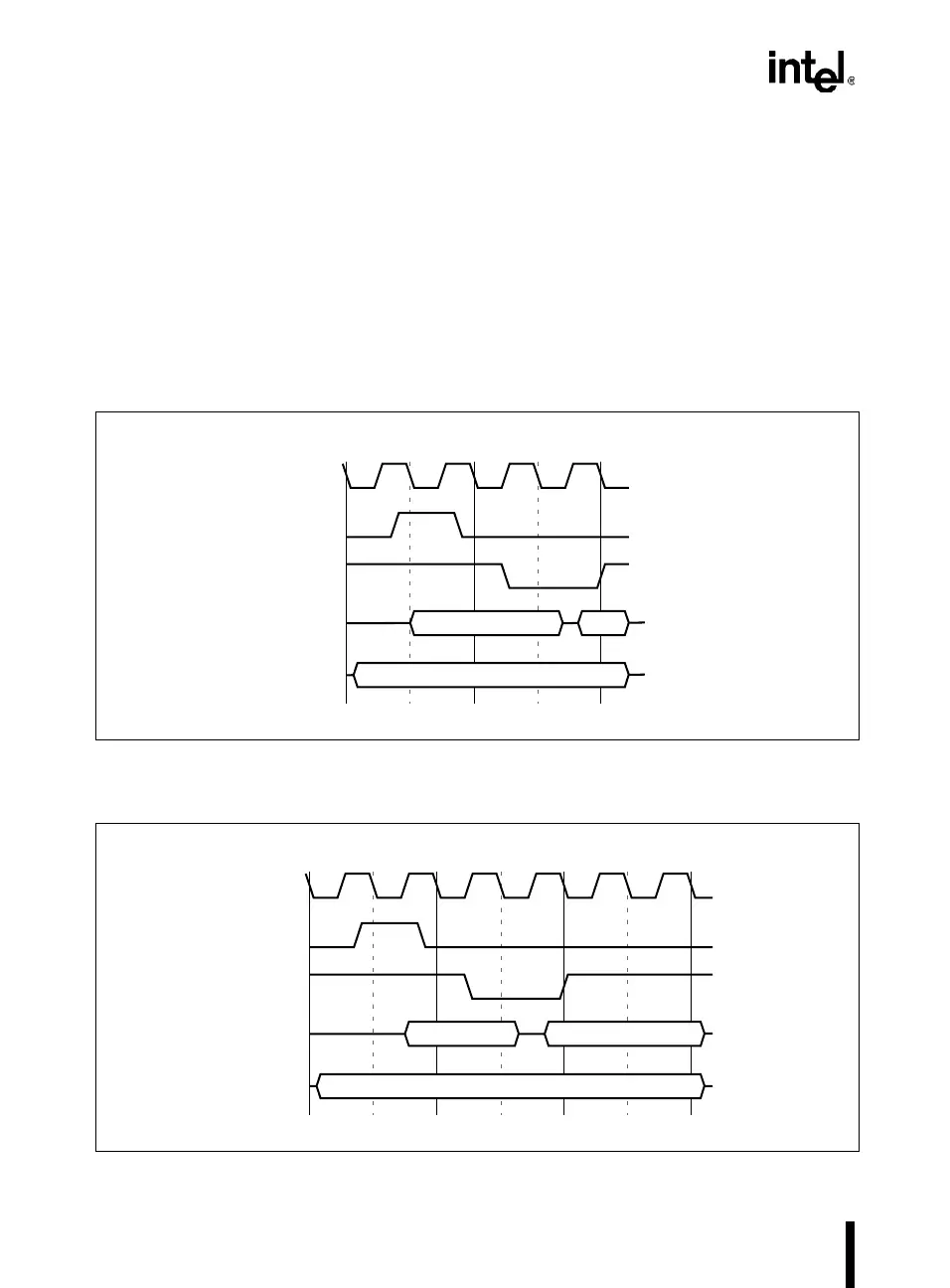
13.2.2 Nonpage Mode Bus Cycles
In nonpage mode, the external bus structure is the same as for MCS 51 microcontrollers. The up-
per address bits (A15:8) are on port 2, and the lower address bits (A7:0) are multiplexed with the
data (D7:0) on port 0. External code read bus cycles execute in approximately two state times.
See Table 13-2 and Figure 13-2. External data read bus cycles (Figure 13-3) and external write
bus cycles (Figure 13-4) execute in approximately three state times. For the write cycle (Figure
13-4), a third state is appended to provide recovery time for the bus. Note that the write signal
WR# is asserted for all memory regions, except for the case of RD1:0 = 11, where WR# is assert-
ed for regions 00:–01: but not for regions FE:–FF:.
Figure 13-2. External Code Fetch (Nonpage Mode)
Figure 13-3. External Data Read (Nonpage Mode)
P0
A17/A16/P2
ALE
RD#/PSEN#
State 1 State 2
XTAL
A2807-04
A7:0
D7:0
A17/A16/A15:8
P0
A17/A16/P2
ALE
RD#/PSEN#
State 1 State 2
XTAL
State 3
A4230-01
A7:0
D7:0
A17/A16/A15:8
i_extmem.fm5 Page 4 Thursday, June 27, 1996 1:39 PM