8XC251SA, SB, SP, SQ USER’S MANUAL
13-6
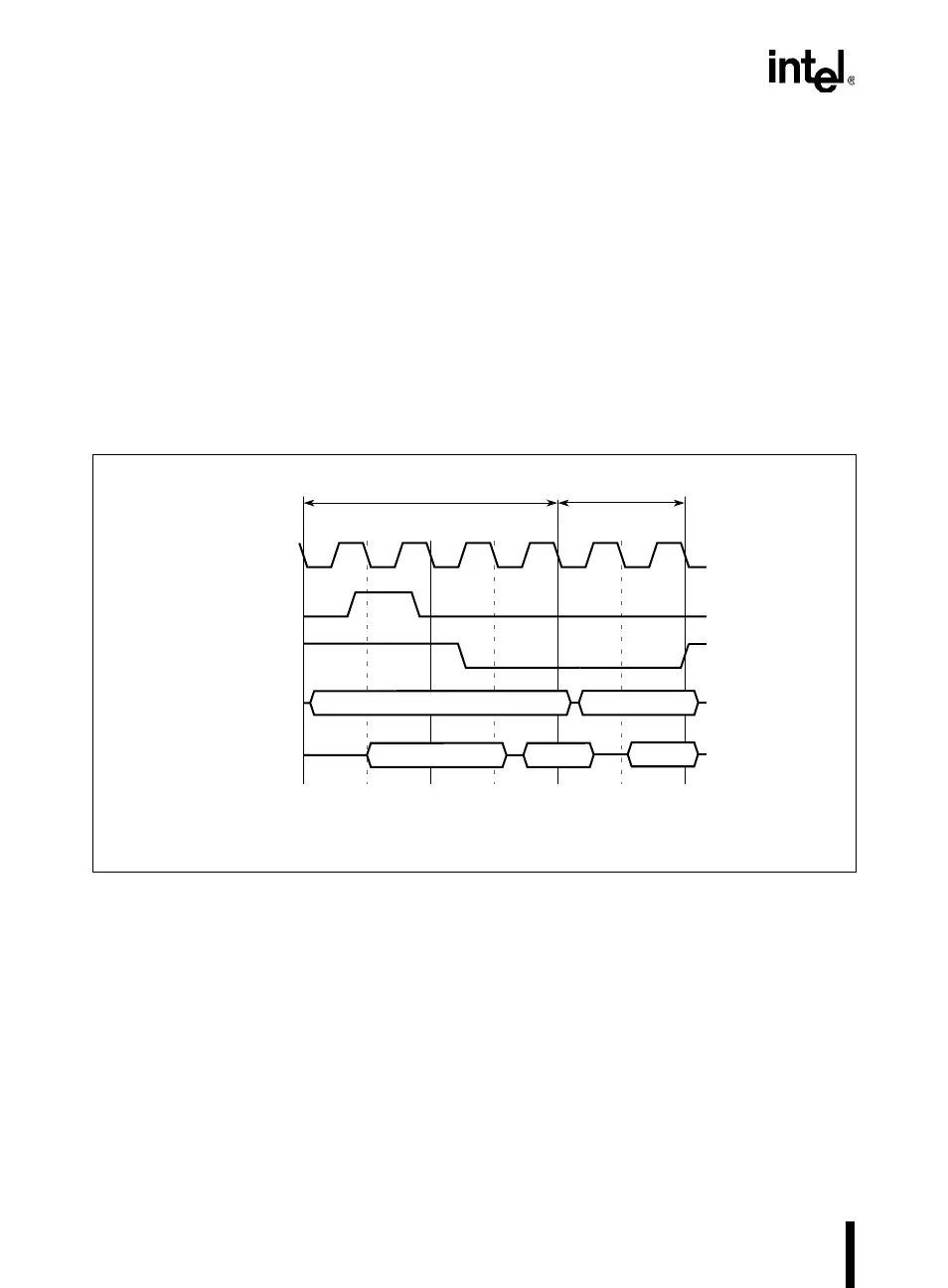
Figure 13-5 shows the two types of external bus cycles for code fetches in page mode. The page-
miss cycle is the same as a code fetch cycle in nonpage mode (except D7:0 is multiplexed with
A15:8 on P2.). For the page-hit cycle, the upper eight address bits are the same as for the preced-
ing cycle. Therefore, ALE is not asserted, and the values of A15:8 are retained in the address
latches. In a single state, the new values of A7:0 are placed on port 0, and memory places the in-
struction byte on port 2. Notice that a page hit reduces the available address access time by one
state. Therefore, faster memories may be required to support page mode.
Figure 13-6 and Figure 13-7 show the bus cycles for data reads and data writes in page mode.
These cycles are identical to those for nonpage mode, except for the different signals on ports 0
and 2.
Figure 13-5. External Code Fetch (Page Mode)
A17/A16/P0
P2
ALE
PSEN#
State 1 State 2
XTAL
State 1
A15:8
A17/A16/A7:0
D7:0
Cycle 1, Page-Miss Cycle 2, Page-Hit
A17/A16/A7:0
D7:0
†
During a sequence of page hits, PSEN# remains low until the end of the last page-hit cycle.
A2809-04
†