13-15
EXTERNAL MEMORY INTERFACE
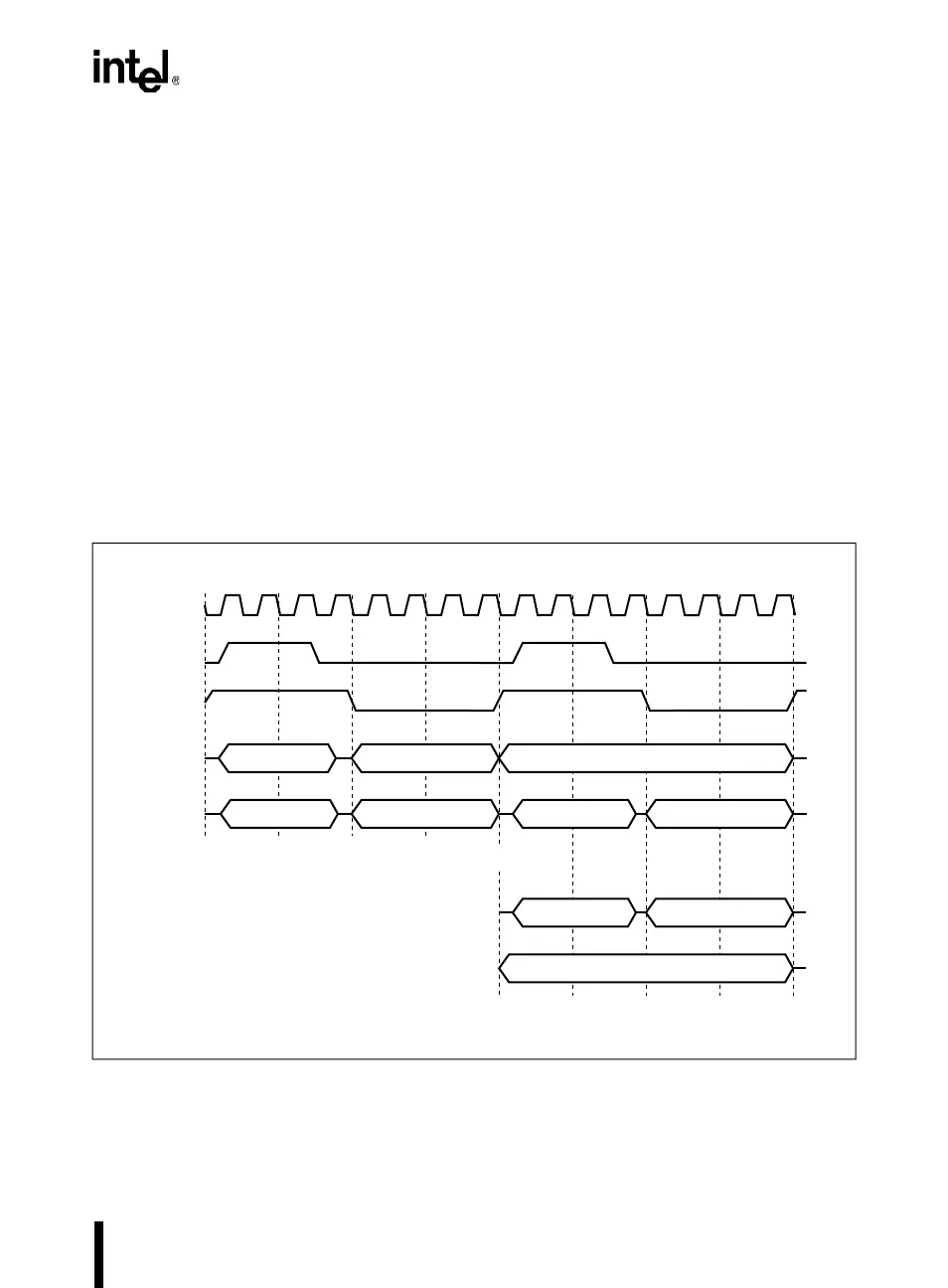
13.6 CONFIGURATION BYTE BUS CYCLES
If EA# = 0, devices obtain configuration information from a configuration array in external mem-
ory. This section describes the bus cycles executed by the reset routine to fetch user configuration
bytes from external memory. Configuration bytes are discussed in Chapter 4, “Device Configu-
ration.”
To determine whether the external memory is set up for page mode or nonpage mode operation,
the 8XC251Sx accesses external memory using internal address FF:FFF8H (UCONFIG0). See
states 1–4 in Figure 13-16. If the external memory is set up for page mode, it places UCONFIG0
on P2 as D7:0, overwriting A15:8 (FFH). If external memory is set up for nonpage mode, A15:8
is not overwritten. The 8XC251Sx examines P2 bit 1. Subsequent configuration byte fetches are
in page mode if P2.1 = 0 and in nonpage mode if P2.1 = 1. The 8XC251Sx fetches UCONFIG0
again (states 5–8 in Figure 13-16) and then UCONFIG1 via internal address FF:FFF9H.
The configuration byte bus cycles always execute with ALE extended and one PSEN# wait state.
Figure 13-16. Configuration Byte Bus Cycles
P0
P2
ALE
PSEN#
XTAL
A7:0 = F8H A7:0 = F8H A7:0 = F8H
A15:8 = FFH D7:0
D7:0
A15:8 = FFH
Nonpage Mode
State 1
A4228-01
State 2 State 3 State 4 State 5 State 6 State 7 State 8
P0
P2
A7:0 = F8H
D7:0
A15:8 = FFH
Page Mode