8XC251SA, SB, SP, SQ USER’S MANUAL
A-2
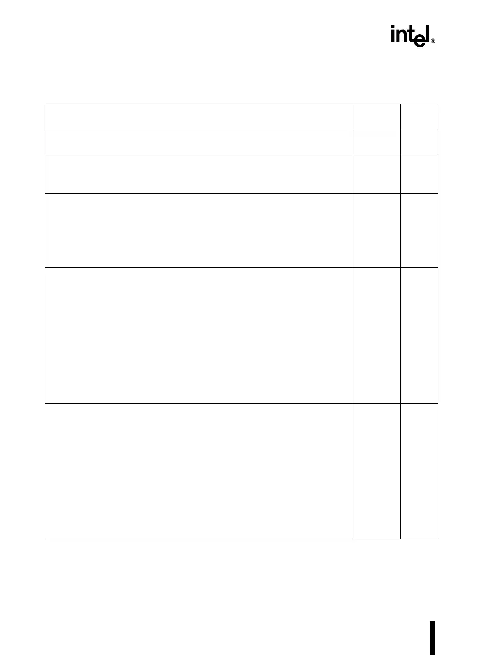
A.1 NOTATION FOR INSTRUCTION OPERANDS
Table A-1. Notation for Register Operands
Register Notation
MCS
®
251
Arch.
MCS 51
Arch.
@Ri A memory location (00H–FFH) addressed indirectly via byte register
R0 or R1
✔
Rn Byte register R0–R7 of the currently selected register bank
n Byte register index: n = 0–7
r r r Binary representation of n
✔
Rm Byte register R0–R15 of the currently selected register file
Rmd Destination register
Rms Source register
m, md, ms Byte register index: m, md, ms = 0–15
s s s s Binary representation of m or md
S S S S Binary representation of ms
✔
WRj Word register WR0, WR2, ..., WR30 of the currently selected register
file
WRjd Destination register
WRjs Source register
@WRj A memory location (00:0000H–00:FFFFH) addressed indirectly
through word register WR0–WR30
@WRj Data RAM location (00:0000H–00:FFFFH) addressed indirectly
+dis16 through a word register (WR0–WR30) + displacement value, where
the displacement value is from 0 to 64 Kbytes.
j, jd, js Word register index: j, jd, js = 0–30
t t t t Binary representation of j or jd
T T T T Binary representation of js
✔
DRk Dword register DR0, DR4, ..., DR28, DR56, DR60 of the currently
selected register file
DRkd Destination Register
DRks Source Register
@DRk A memory location (00:0000H–FF:FFFFH) addressed Indirectly
through dword register DR0–DR28, DR56, DR60
@DRk Data RAM location (00:0000H–FF:FFFFH) addressed indirectly
+dis24 through a dword register (DR0–DR28, DR56, DR60) + displacement
value, where the displacement value is from 0 to 64 Kbytes
k, kd, ks Dword register index: k, kd, ks = 0, 4, 8, ..., 28, 56, 60
u u u u Binary representation of k or kd
U U U U Binary representation of ks
✔