B-3
SIGNAL DESCRIPTIONS
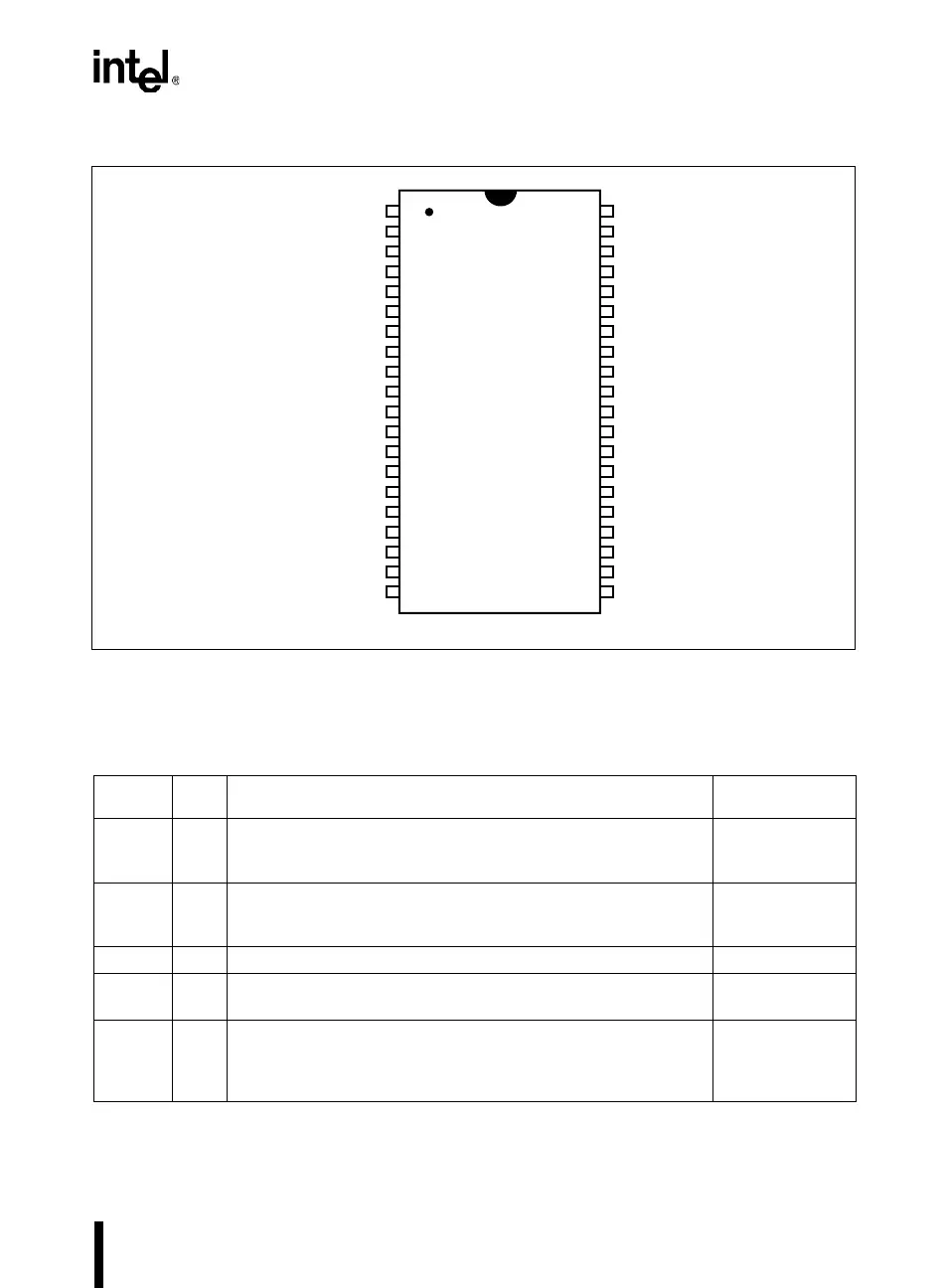
Figure B-2. 8XC251SA, SB, SP, SQ 40-pin PDIP and Ceramic DIP Packages
Table B-2. Signal Descriptions
Signal
Name
Type Description
Alternate
Function
A17 O Address Line A17. Eighteenth external address bit (A17) in
extended bus applications. Selected by configuration byte
UCONFIG0, bits RD1:0 (Table B-3). Also see RD# and PSEN#.
P1.7/CEX4/
WCLK
A16 O Address Line A16. Seventeenth external address bit (A16) in
extended bus applications. Selected by configuration byte
UCONFIG0, bits RD1:0 (Table B-3). Also see RD#.
P3.7/RD#
A15:8
†
O Address Lines. Upper address lines for the external bus. P2.7:0
AD7:0
†
I/O Address/Data Lines. Multiplexed lower address lines and data
lines for external memory.
P0.7:0
ALE O Address Latch Enable. ALE signals the start of an external bus
cycle and indicates that valid address information is available on
lines A15:8 and AD7:0. An external latch can use ALE to
demultiplex the address from the address/data bus.
PROG#
†
The descriptions of A15:8/P2.7:0 and AD7:0/P0.7:0 are for the nonpage mode chip configuration (com-
patible with 44-pin PLCC and 40-pin DIP MCS
®
51 microcontrollers). If the chip is configured for page
mode operation, port 0 carries the lower address bits (A7:0), and port 2 carries the upper address bits
(A15:8) and the data (D7:0).
1
2
3
4
5
6
7
8
9
10
11
12
13
14
15
16
17
18
19
20
V
CC
AD0 / P0.0
AD1 / P0.1
AD2 / P0.2
AD3 / P0.3
AD4 / P0.4
AD5 / P0.5
AD6 / P0.6
AD7 / P0.7
EA# /
V
PP
ALE / PROG#
PSEN#
A15 / P2.7
A14 / P2.6
A13 / P2.5
A12 / P2.4
A11 / P2.3
A10 / P2.2
A9 / P2.1
A8 / P2.0
P1.0 / T2
P1.1 / T2EX
P1.2 / ECI
P1.3 / CEX0
P1.4 / CEX1
P1.5 / CEX2
P1.6 / CEX3 / WAIT#
P1.7 / CEX4 / A17 / WCLK
RST
P3.0 / RXD
P3.1 / TXD
P3.2 / INT0#
P3.3 / INT1#
P3.4 / T0
P3.5 / T1
P3.6 / WR#
P3.7 / RD# / A16
XTAL2
XTAL1
V
SS
40
39
38
37
36
35
34
33
32
31
30
29
28
27
26
25
24
23
22
21
8XC251SA
8XC251SB
8XC251SP
8XC251SQ
View of
component
as mounted
on PC board
A4206-03