Goodrive300-LIFT series inverter Expansion cards
-142-
1
5
6
11
10
15
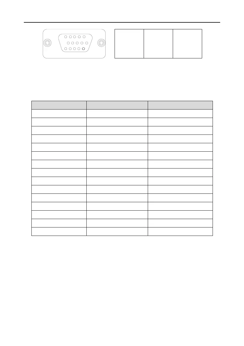
TER-OA TER-OB COM1
DB15
Frequency division output
1
5
6
11
10
15
TER-OA TER-OB COM1
DB15
分频输出接口
Figure A-12 PG card wire port and wire terminals
TER-OA, TER-OB and COM1 are the signal terminals of frequency division output.
Note: PE terminal in PG card are not grounded to the earth, so users can grounding it by themselves.
DB15 is the port of the encoder input signal. The sequence of the ports signal is as below:
When using the synchronous PG card, it is necessary to insert the connecting wire of SIN/COS or
UVW whose signal array is corresponding with PG card into DB15 of PG card.
The frequency division coefficient is determined by the dial switch on the card. The dial switch
consists of 8 bits. The frequency division is decided by the value of the binary digits (at dial switch)
plus 1. The bit marked as "1" on the DIP switch is the lower binary bit, while "8" is the higher binary bit.
When the dial switch is switched to ON, the bit is valid, indicating "1"; otherwise, it is invalid, and it is
indicating "0".
 Loading...