15
In order to prevent a malfunction caused by interference voltage on the
control inputs, the following steps should be observed:
• Establish a common ground point for all ground connec-
tions.
• Use shielded cable with twisted pair wires.
• Terminate shield wires to earth ground,
only at inverter.
• Separate control and power wires 8" or more apart.
• Control and power wires to cross at a right angle.
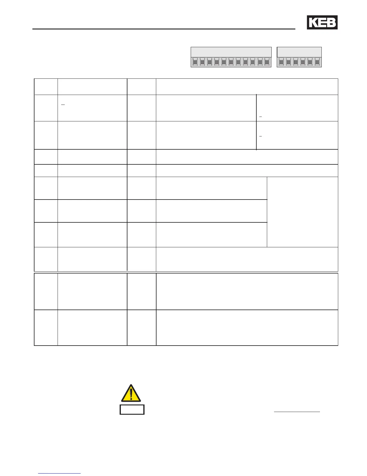
PIN Function Name Description
1 + Analog input 1 AN1 Voltage input for speed resolution: 11 Bit, 0...±10 VDC
^ 0...±CP.11, scan time: 2 ms
5 Analog output 1 ANOUT1 Analog output of the actual voltage range: 0...±10 VDC
output frequency ^ 0...±100 Hz, Rout = 100 kΩ,
resolution: 12bit
7 +10V Output CRF Analog supply voltage for speed ref. +10 VDC +5%, max. 4 mA
8 Analog Common COM Common for analog In- and Outputs
10 Fixed frequency 1
I 1 I1 + I2 = Fixed frequency 3;
11 Fixed frequency 2 I 2 no input = analog voltage (speed) ref.
14 Forward F Preset rotation; Ri = 2.1 k Ohm
15 Reverse R Forward has priority
scan time: 2 ms
16 Control release, Reset ST Inverter enable, disable;
Error Reset at opening
20 24V-Output Vout Approx. 24V Output (max.100 mA)
22 Digital Common 0V Common for digital In-/Outputs
24 Relay 1, NO contact RLA Relay output;
25 Relay 1, NC contact RLB fault relay(default);
26 Relay 1, switching cont. RLC Function can be changed with CP.31; max. 30 V DC, 1 A
27 Relay 2, NO contact FLA Relay output;
28 Relay , NC contact FLB frequency dependent switch (default);
29 Relay 2, switching cont. FLC Function can be changed with CP.32; max. 30 V DC, 1 A
Installation and Connection
3.4.2 Connection
of the control
signals
 Loading...