Page1.3 - 4 COMBIVERT R6-N © KEB, 2015-07
Hardware
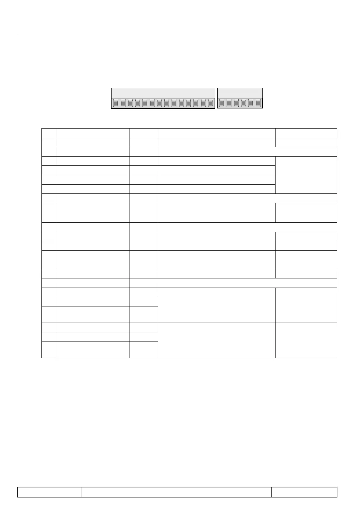
X2A
10 11 12 13 14 15 16 17 18 19 20 21
22 23 24 25 26 27 28 29
Core cross-section 0.14…1.5 mm², tightening torque 0.5 Nm
PIN Function Name Description Specications
10 24 V DC input Uin External supply of the control board 21,6…26,4 V DC / 1A
11 Mass COM Reference potential
12 Digital input 1 ST Control release / reset
Ri:4.4kΩ
13 Digital input 2 I1 programmable
14 Digital input 3 I2 programmable
15 Digital input 4 I3 programmable
16 Mass COM Reference potential
17 24V-output Uout Voltage supply for in- and outputs
approx. 24 V / max.
100 mA
18 Mass COM Reference potential
19 Digital output 1 O1 Transistor output (DC > CP.19) I
max:25mA
20 Digital output 2 O2 Transistor output (error message) I
max:25mA
21 Analog output 1 / gain ANOUT
Difference between actual supply fre-
quency and set supply frequency
1 V per 0,1 Hz differ-
ence
22 24Voutput Uout see terminal 17
23 Mass COM Reference potential
24 Relay 1 / NO contact RLA
Relay output
Ready signal (no error)
max. 30 V DC *)
0.01…2 A DC
25 Relay 1 / NC contact RLB
26
Relay 1 / switching
contact
RLC
27 Relay 2 / NO contact FLA
Relay output
(DC > CP.19 and tightened load-shunt)
max. 30 V DC *)
0.01…2 A DC
28 Relay 2 / NC contact FLB
29
Relay 2 / switching
contact
FLC
*) The relay outputs must be operated with max. 48 V DC protective separation voltage to guarantee the CE
standard. After consultation KEB a current of max. 1 A DC is permissible for 120 V AC.
 Loading...