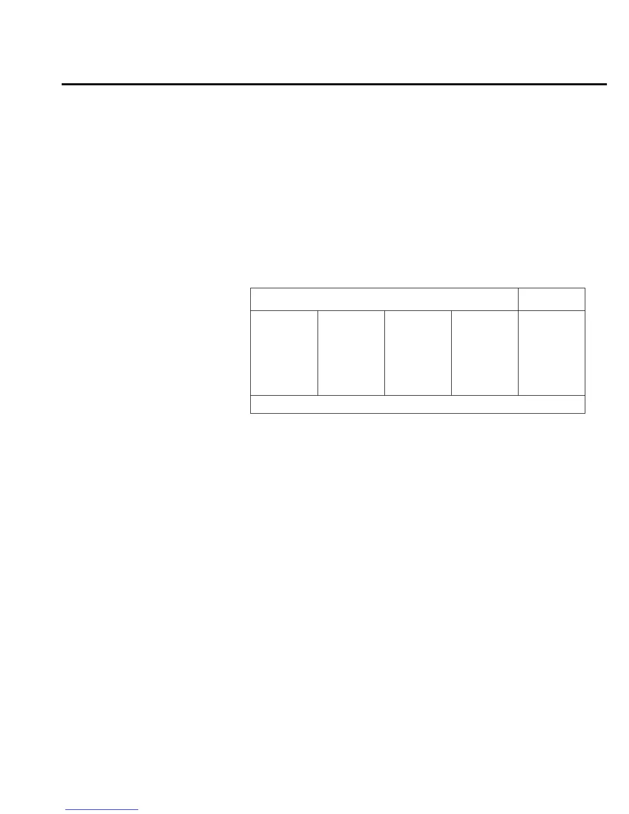
Test 200.2 — REFERENCE
Bank REF/MUX
Inputs Open
Expected Value 10 volts
Limits 1 volt
Fault Message AD X100
Description
Same as test 200.1 except the A/D MUX is configured for
×
100 gain (/
×
100 control line is low). The gain path is through U129 pin 10 to 11. Resis-
tor network R271 is used to configure the x100 gain. Measure 10V at AD_IN.
Bit patterns
Bit pattern Register
QQ
87654321
—U106—
110v1111
QQ
87654321
—U109—
00101111
QQ
87654321
—U134—
1v10000v
—U130—
10001011
QQ
87654321
—U121—
01110010
ACDC_STB
MUX_STB
IC pins: Q8=11, Q7=12, Q6=13, Q5=14, Q4=7, Q3=6, Q2=5, Q1=4
Troubleshooting 2-29