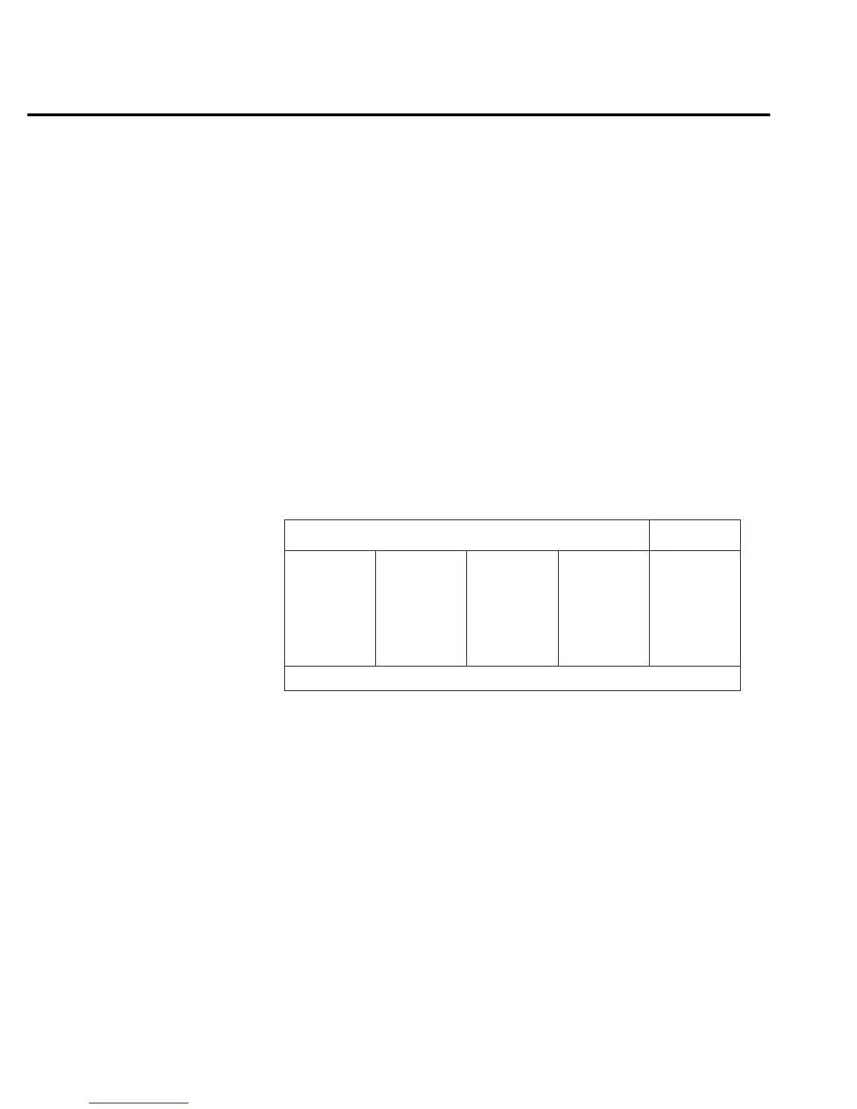
TEST BANK: REF/MUX
Test 200.1 — REFERENCE
Bank REF/MUX
Inputs Open
Expected Value 1 volt
Limits 0.1 volts
Fault Message 1VREF/AD X10
Description
The 7V REFHI signal is routed through R189 and R185, which forms a
0.014/1 voltage divider with R188. The 0.1V result (0.014
×
7V = 0.1V) is
then applied to S1 of U163. The A0, A1 and A2 bit pattern on U163 is set to
connect the S1 signal (0.1V) to the D output. The signal is then routed
through R159, Q117 and R166 to the non-inverting input of op amp U166.
A/D MUX (U166) is configured for
×
10 gain (/
×
10 control line is low turning
on U129 analog switch; pins 6 to 7). Feedback resistors R309 and R310 con-
figure the
×
10 gain. Measure 1V at AD_IN.
Bit patterns
Bit pattern Register
QQ
87654321
—U106—
110v1111
QQ
87654321
—U109—
00101111
QQ
87654321
—U134—
1v10000v
—U130—
10000111
QQ
87654321
—U121—
01110010
ACDC_STB
MUX_STB
IC pins: Q8=11, Q7=12, Q6=13, Q5=14, Q4=7, Q3=6, Q2=5, Q1=4
2-28 Troubleshooting