Test 201.1 — A/D MUX LO
Bank REF/MUX
Inputs Open
Expected Value 0 volts
Limits 0.0001 volts
Fault Message SENSE LO 0
Description
Signal LO is routed through R181 and Q122 (/LOMUXA control line
high) into unity gain amp U126. Signal LO is then routed to S7 of U163. The
A0, A1 and A2 bit pattern on U163 connects S7 to the D output, which then
routes signal LO through Q117 to U166.
The A/D MUX (U166) is configured for
×
1 gain (/
×
1 control line low) by
closing U129; pin 2 to 3. Measure 0V at AD_IN.
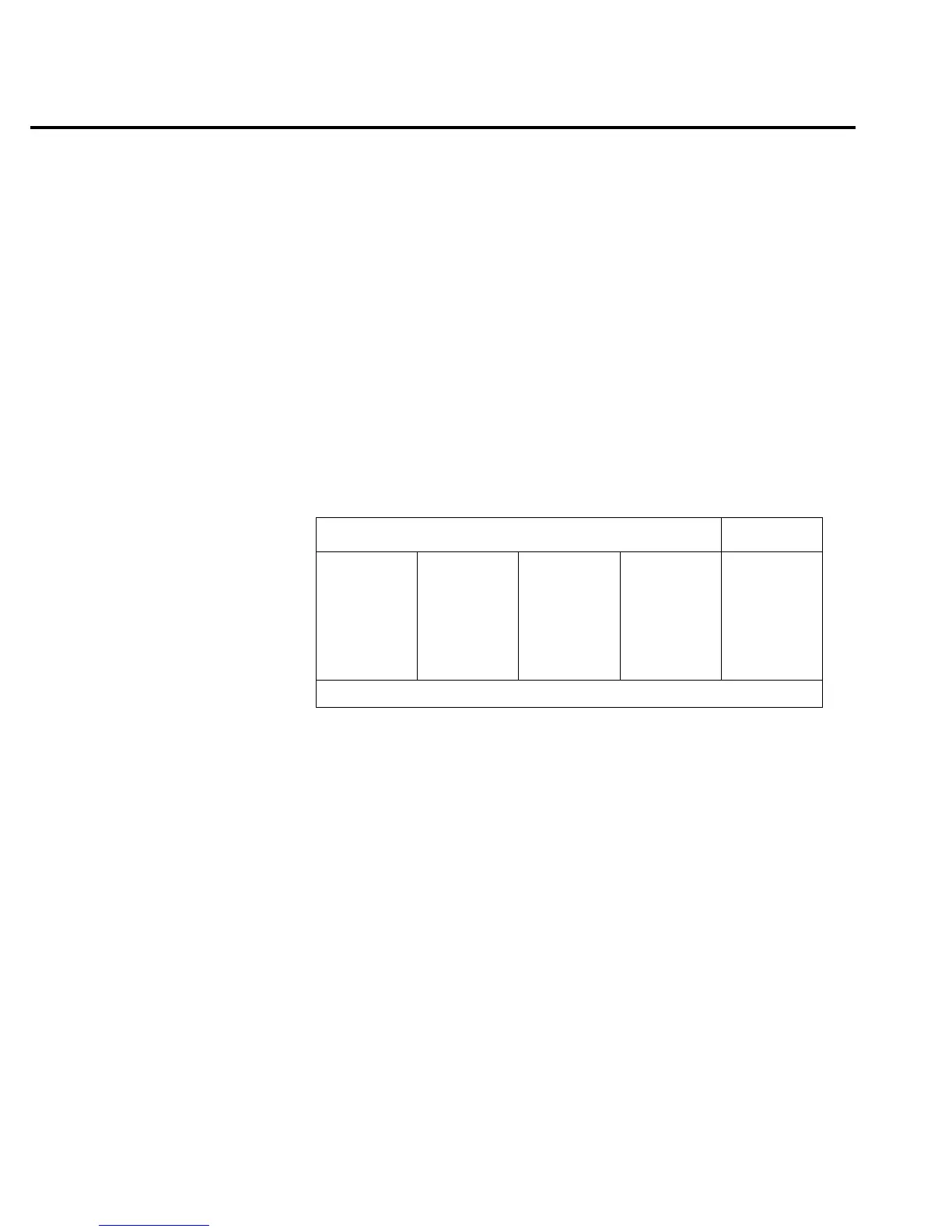
Bit patterns
Bit pattern Register
QQ
87654321
—U106—
110v1111
QQ
87654321
—U109—
00101111
QQ
87654321
—U134—
1v10000v
—U130—
11011101
QQ
87654321
—U121—
01110010
ACDC_STB
MUX_STB
IC pins: Q8=11, Q7=12, Q6=13, Q5=14, Q4=7, Q3=6, Q2=5, Q1=4
2-30 Troubleshooting