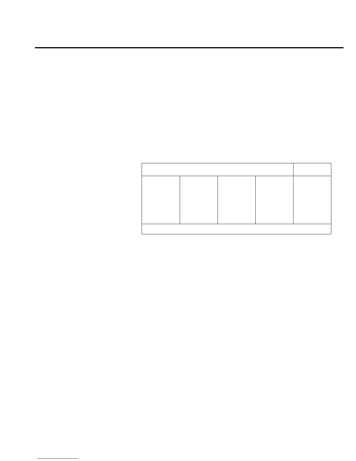
Test 201.2 — A/D MUX LO
Bank REF/MUX
Inputs Open
Expected Value 0 volts
Limits 0.0001 volts
Fault Message MUX LO
Description
This test is similar to test 201.1, except signal LO is routed through R274
to S8 of U163. Signal LO is then routed through Q117 to U166, which is con-
figured for
×
1 gain. Measure 0V at AD_IN.
Bit patterns
Bit pattern Register
QQ
87654321
—U106—
110v1111
QQ
87654321
—U109—
00101111
QQ
87654321
—U134—
1v10000v
—U130—
11111101
QQ
87654321
—U121—
01110010
ACDC_STB
MUX_STB
IC pins: Q8=11, Q7=12, Q6=13, Q5=14, Q4=7, Q3=6, Q2=5, Q1=4
Troubleshooting 2-31