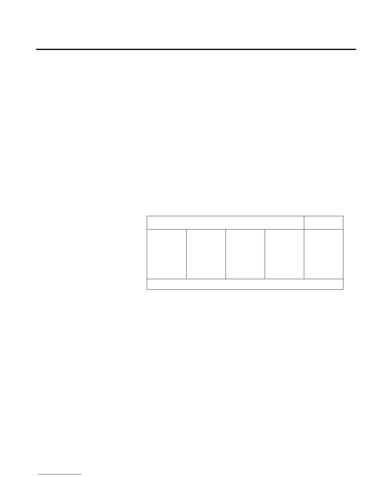
Test 302.1 — 2W SENSE
Bank DC/OHM
Inputs Open
Expected Value 7 volts
Limits 0.7 volts
Fault Message 2W SENSE 7V
Description
The +7V reference is again switched to REFBOOT, and routed through
R272, Q109, the 9.9M
Ω
half of divider R117, the parallel combination of
R115, R324 and L109, and then through R113, R107, R103, R108, and
K101. At this point, the reference is labeled 2WSEN_I.
Reference 2WSEN_I is then routed through K102 (control line SETK1
high) to the 2WSEN_O node. This node then goes through Q105 (2W control
line high), to U113 (BUFCOM) and to the A/D MUX with
×
1 gain. Measure
+7V at AD_IN.
Bit patterns
Bit pattern Register
QQ
87654321
—U106—
110v1111
QQ
87654321
—U109—
00011111
QQ
87654321
—U134—
0v10000v
—U130—
10111101
QQ
87654321
—U121—
10000010
ACDC_STB
MUX_STB
IC pins: Q8=11, Q7=12, Q6=13, Q5=14, Q4=7, Q3=6, Q2=5, Q1=4
Troubleshooting 2-35