Test 301.2 — HI OHMS
Bank DC/OHM
Inputs Open
Expected Value 12.4 volts
Limits 0.5 volts
Fault Message 13.3 REFBOOT
Description
This test is the same as 301.1 except that the +13.3V ohms reference is
tested. The +13.3V reference is generated by the same circuit as the +7V ref-
erence. 14V is routed through Q130 and then applied to a 1K/10K divider
which is part of R271. The +13.3V divider output is routed through analog
switch U133 (/.7V control line low) to op amp U123. The remainder of the
path is the same as test 300.1.
The expected voltage at AD_IN would be +13.3V except that at the source
lead of Q104 (labeled SOURCE) there is a clamping circuit. Back-to-back
11V zener diodes VR105 and VR106, and photo-coupler U107 clamp the
voltage at the SOURCE node to about +12.4V. Measure +12.4V at AD_IN.
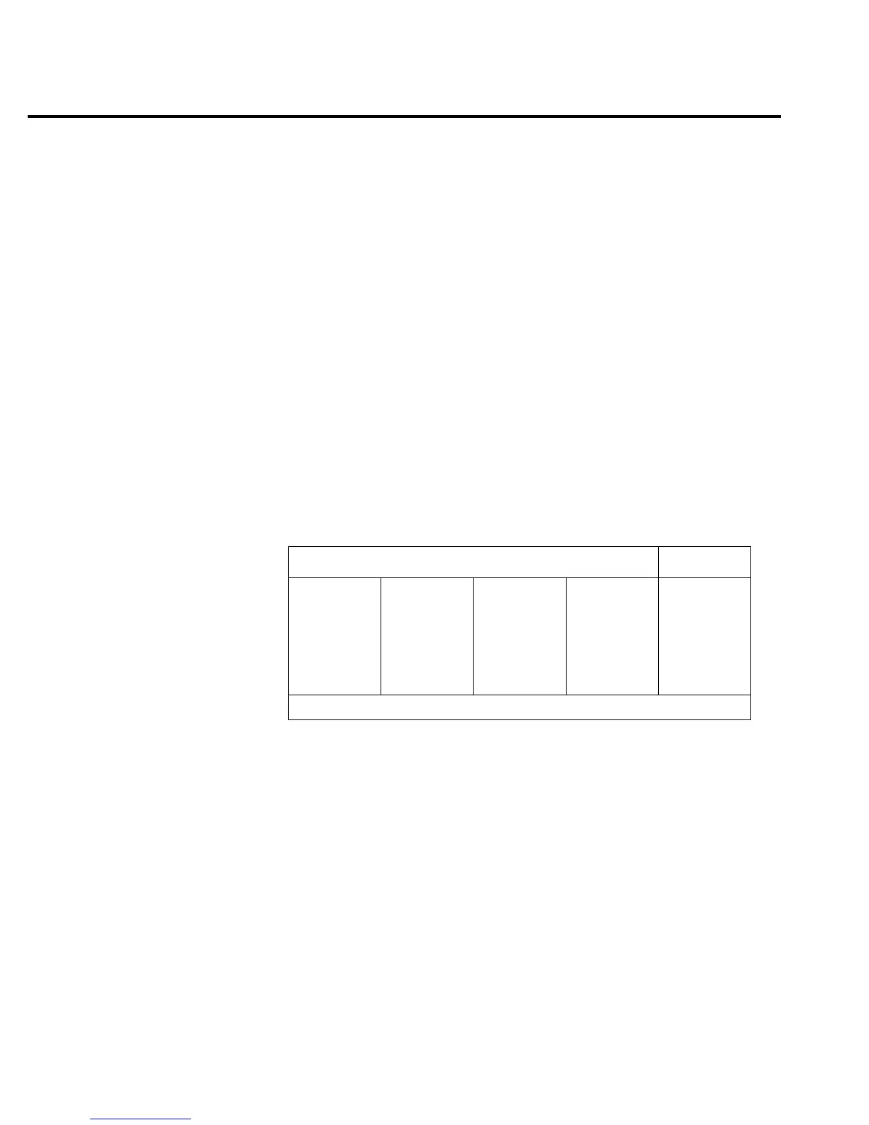
Bit patterns
Bit pattern Register
QQ
87654321
—U106—
110v1111
QQ
87654321
—U109—
00101111
QQ
87654321
—U134—
0v01001v
—U130—
10111101
QQ
87654321
—U121—
10000100
ACDC_STB
MUX_STB
IC pins: Q8=11, Q7=12, Q6=13, Q5=14, Q4=7, Q3=6, Q2=5, Q1=4
2-34 Troubleshooting