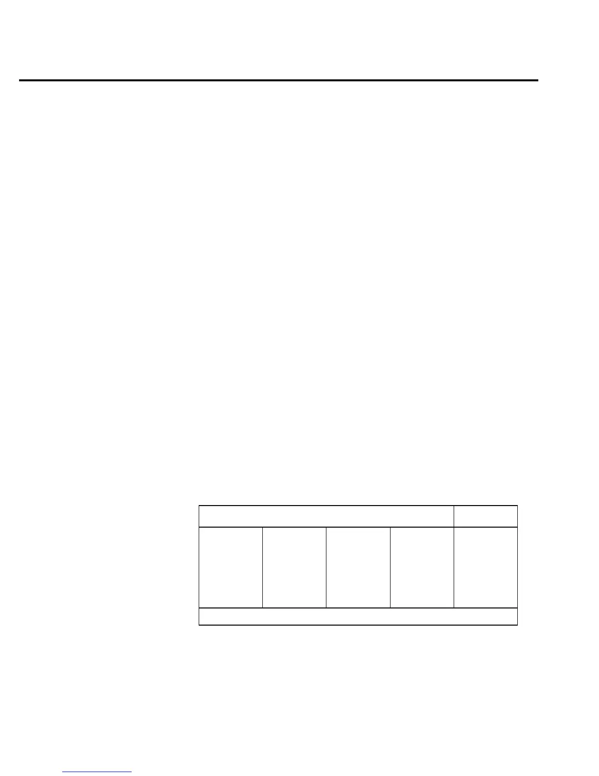
Test 403.2 — NON INV BEX2
Bank VAC
Inputs Open
Expected Value 1.08 volts
Limits? 0.2 volts
Fault Message NON INV BEX2
Description The previous test sets up the circuit for this test. There is a routine in soft-
ware that generates a waveform for the ACV tests. This is done by selecting
the 13.3V reference by closing analog switch U133 (/.7V control line low).
The reference is buffered by U123 is labeled REFBOOT.
The REFBOOT signal is switched into the front end through Q109 via
U120 by toggling the /HIOHM line. This switching routine is done in firm-
ware. Q114 and Q136 are turned ON (conducting to ground) by U120 (DIV-
LO control line low). The 100kΩ leg of R117 acts as a pull-up and pull-down
to clean up the switched signal REFBOOT.
The signal path continues through Q101, Q102 and K101 to ACIN. The
switched ACIN signal (coupled across C105) is applied to the circuit de-
scribed in test 403.1 and the measurement is made.
The input signal switching stops while the A/D takes the reading. Signal
switching continues after the reading is done. There are delays before the
reading is taken to ensure that the ACV section and filters have enough time
to reach a charged full scale reading. In this phase, the switched signal can
be traced through the circuit described in test 403.1. Measure 1.08V DC at
A/D_IN.
Bit patterns
Bit pattern Register
QQ
87654321
—U106—
011v0011
QQ
87654321
—U109—
11011111
QQ
87654321
—U134—
1v01000v
—U130—
10011101
QQ
87654321
—U121—
01110000
ACDC_STB
MUX_STB
IC pins: Q8=11, Q7=12, Q6=13, Q5=14, Q4=7, Q3=6, Q2=5, Q1=4
2-50 Troubleshooting

 Loading...