SERVICE MANUAL
KEMPACT RA_V_1.2
16 (40)
Kemppi Oy
3.2.3.6. PFC Boost control circuitry
• PFC control circuitry is located on the primary side. Auxliary transformer T003 supplies operating voltage for the PFC
control circuitry. The output voltage of the T003 is first rectified and then linear regulator is used to regulate auxiliary
voltage to 15V. PFC control IC N1 regulates DC-link voltage to approximately 370V
3.3. Main circuit diagram 253-, 323-models
3.3.1. Main circuit card Z001
3.3.1.1. EMC filter
• Capacitors C5 - C7, C8 - C10, C19 - C21 and inductors T4 and L1 form an EMC filter
• First part of the filter is three phase filter which is located before the three phase rectifier V2
• Second part is DC filter (L1) which is located after three phase rectifier
3.3.1.2. Inrush current limiting
• PTC resistor R1 limits inrush current when the power source is switched on
• R1 is bypassed with relays K1 and K2 after DC link capacitors C17, C18 have been charged
• Relays K1 and K2 are controlled with the microcontroller
3.3.1.3. IGBT driver
• IGBT driver consists of gate transformers T2 and T3 and surrounding components
3.3.1.4. Current transformer T1
• Current transformer T1 is monitoring primary current and stops power stage operation if current is raising too high
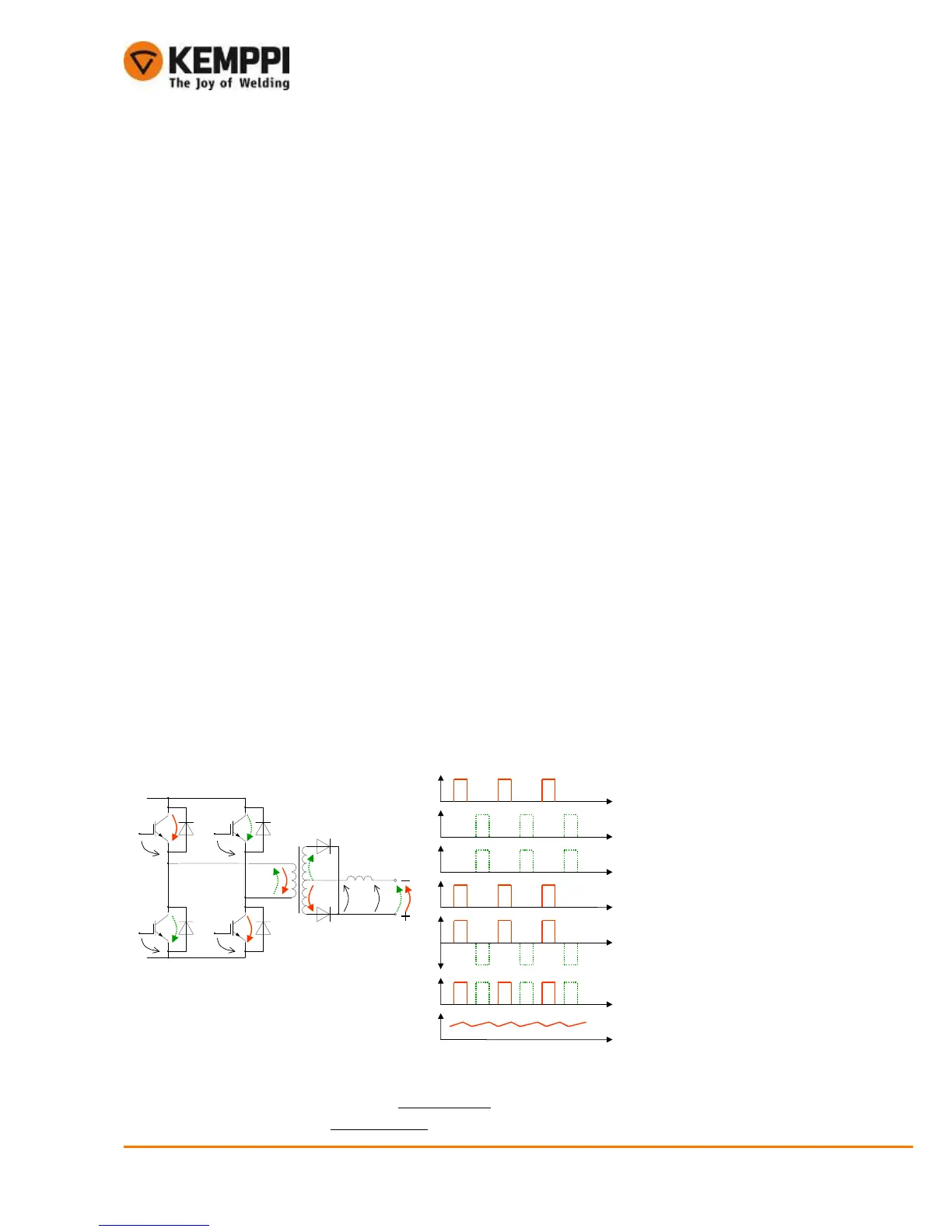
3.3.1.5. Main circuit
• Main circuit topology is H-bridge. The H-bridge topology requires four power switches which are implemented using
IGBT module V2. The switching frequency of the H – bridge is 20 kHz
• 253 power source uses 50A module
• 323 power source uses 75A module
G1
G3
U
G4
U
U
G5
U
L1
G1
G3
G4
G2
T1
G5
L1
When IGBT-transistors G1 and G4 conduct, there is a positive voltage U
T1
in main transformer T1 primary and when IGBT-
transistors G2 and G3 conduct there is a negative voltage U
T1
in main transformer primary. Power is adjusted by changing the
IGBT timings (PWM).
 Loading...