Page 25
Find us at www.keysight.com
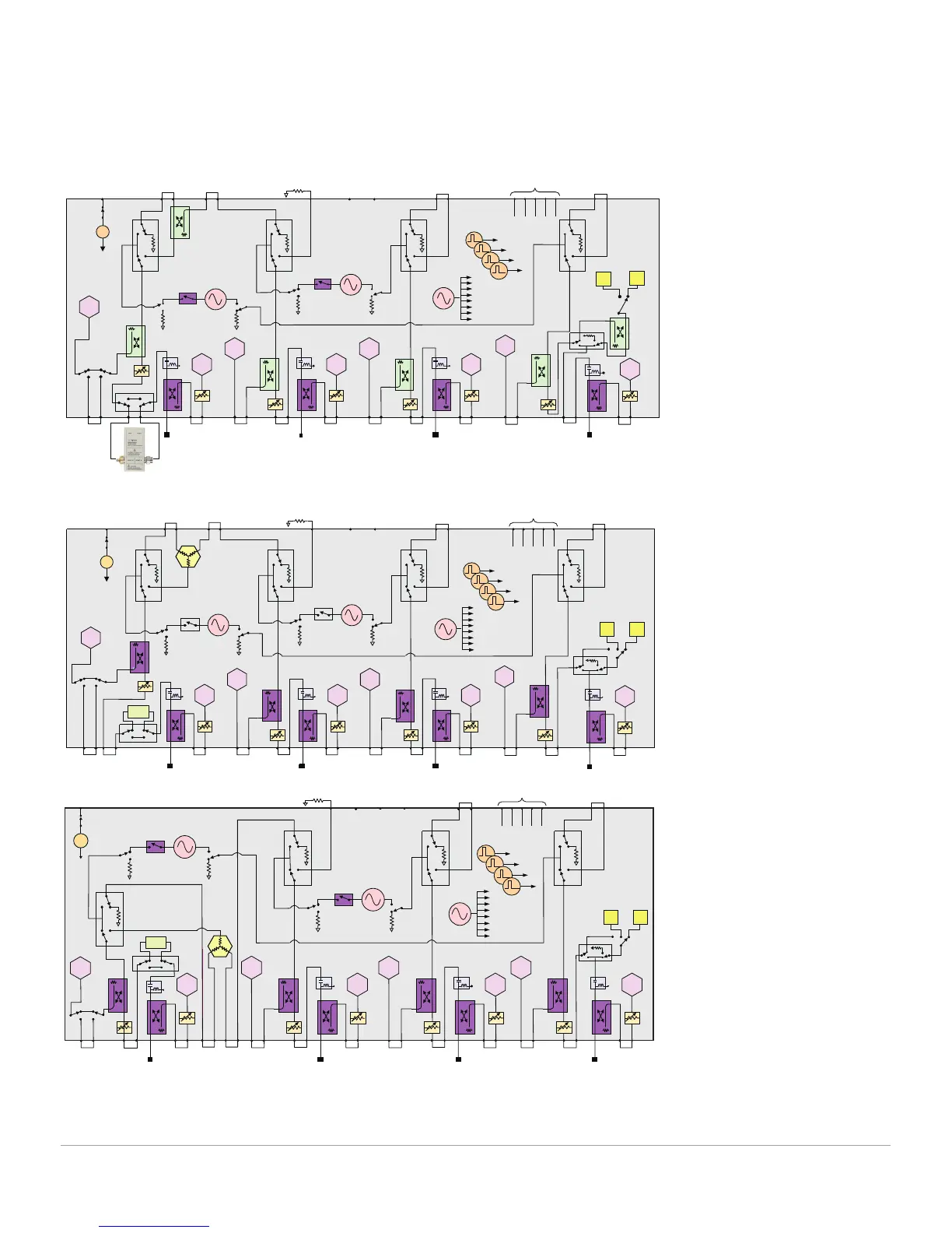
C
R3
Test port 1
R1
Test port 4
R4
A
D
Rear panel
Pulse generators
1
2
3
4
Source 1
OUT 1 OUT 2
Pulse
modulator
Source 2
OUT 1 OUT 2
Pulse
modulator
Test port 2
R2
B
Noise receiver
10 MHz -
6 GHz
6-8.5/
13.5/
26.5 GHz
To receivers
LO
+28 V
Test port 3
Signal
combiner
+
-
Impedance tuner for noise
figure measurements
J9J10J11 J8 J7 J2 J1J4 J3
35 dB 35 dB 35 dB
35 dB
65 dB
65 dB
65 dB
65 dB
J6 J5
RF
OUT
LO
OUT
R A B C D
IF inputs
C
R3
Test port 1
R1
Test port 4
R4
A
D
Rear panel
Pulse generators
1
2
3
4
Source 1
OUT 1 OUT 2
Pulse
modulator
Source 2
OUT 1 OUT 2
Pulse
modulator
Test port 2
R2
B
Noise receiver
10 MHz-
6 GHz
6 -43.5/
50 GHz
To receivers
LO
+28V
Test port 3
Signal
combiner
+
-
J9J10J11 J8 J7 J2 J1J4 J3
35 dB 35 dB 35 dB
35 dB
60 dB
60 dB
60 dB
J6 J5
RF
OUT
LO
OUT
R A B C D
IF inputs
60 dB
Tuner
N5241/42/49B 4-port
block diagram with
noise figure option
1
N5244/45B 4-port
block diagram with
noise figure option
1
N5247B 4-port
block diagram with
noise figure option
1
Test port 3
C
R3
Test port 1
R1
Test port 4
R4
Test port 2
R2
A
D
B
To receivers
LO
Pulse generators
Rear panel+28 V
1
2
3
4
OUT 2
Source 1
OUT 1
Pulse
modulator
+
-
Source 2
(standard)
OUT 1 OUT 2
Pulse
modulator
J12 J6 J5J7 J2 J1J4 J3
50
dB
50 dB
50 dB
50 dB
50 dB 50 dB 50 dB 50 dB
RF2
OUT
RF1
OUT
LO
OUT
Signal
combiner
R A B C D
Noise receivers
10 MHz -
6 GHz
6 -50
GHz
Tuner
1. S93029B/A software is required to control the impedance tuner and tuner switch at port one, and the noise
receiver and noise switch at port two.
PNA Family Applications and Options (Continued)
PNA-X block diagrams with noise figure option
 Loading...