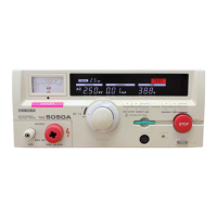
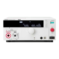
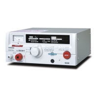
6-22 TOS5051A/5050A
SIGNAL I/O Specifications
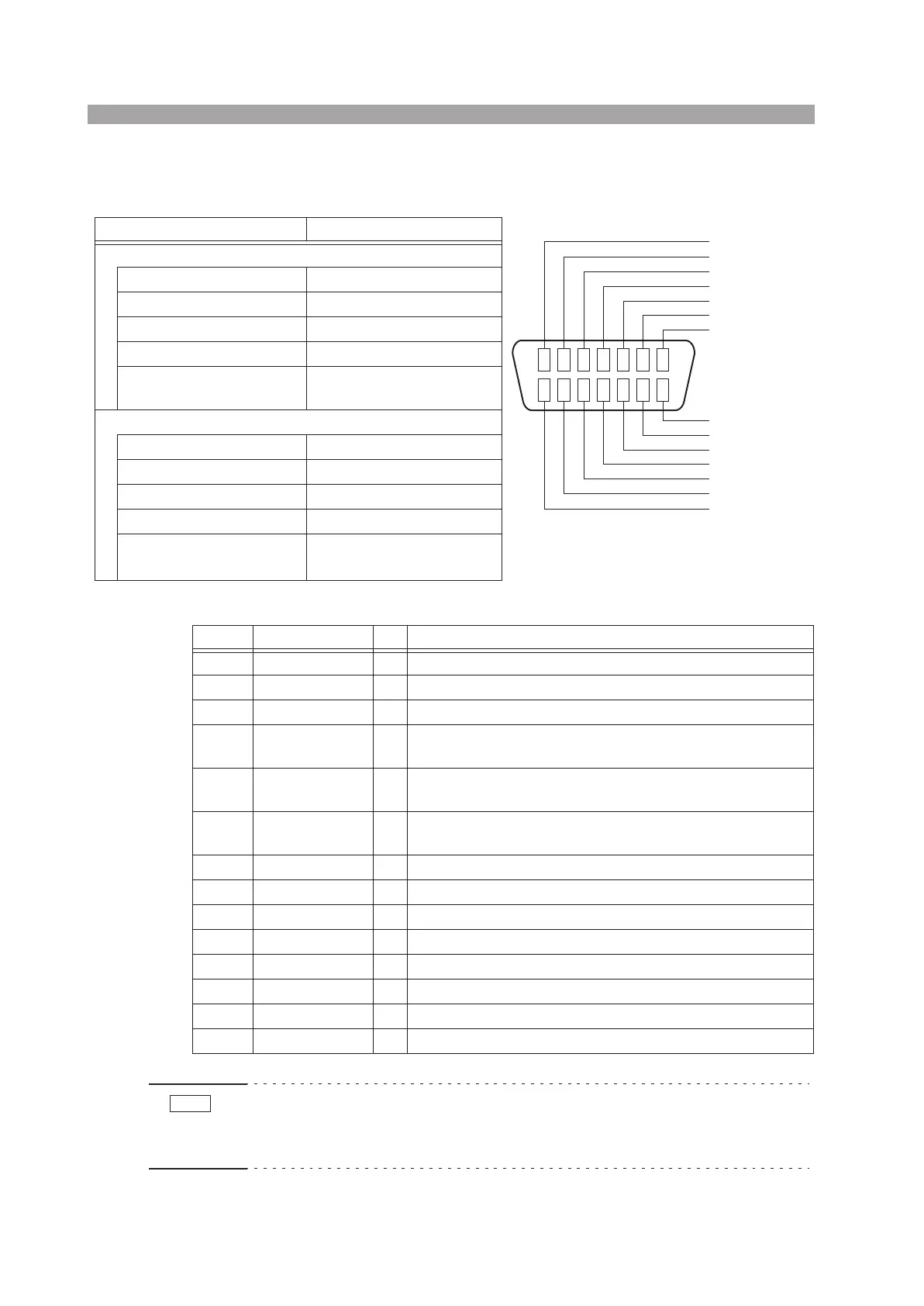
Table6-1 Specifications of the SIGNAL I/O Signals
Table 6-2 SIGNAL I/O pin assignments
• * The Interlock signal input pin assignments are different from the old model
TOS5050/5051. To use the Amphenol plug for the old model to this tester, you
have to change the wiring between pins 9 and 14 to the wiring pins 1 and 9.
Item Specifications
Input signal control section
High-level input voltage 11 V to 15 V
Low-level input voltage 0 V to 4 V
Low-level input current -5 mA maximum
Input time width 5 ms minimum
Isolation type
Photocoupler
(30 VDC/30 VACrms MAX)
Output signal control section
Type of output Open collector output
Output withstanding voltage 30 VDC
Output saturation voltage Approx. 1.1 V, at 25 ˚C
Maximum output current 400 mA (in total)
Isolation
Photocoupler
(30 VDC/30 VACrms MAX)
Fig.6-1 SIGNAL I/O Connector
Pin layout
Pin No. Signal I/O Output condition and signal description
1 INTERLOCK+ I Interlock signal input pin*
2 H.V ON O ON while high voltage is applied across the output terminals
3 TEST O ON while the test is in progress
4 PASS O
ON for approximately 0.2 s when PASS results from judgment.
ON continuously when PASS HOLD is enabled.
5 U FAIL O
ON continuously when a current above the upper cutoff current
is detected and FAIL results from judgment.
6 L FAIL O
ON continuously when a current below the lower cutoff current
is detected and FAIL results from judgment.
7 READY O ON when ready
8 PROTECTION O ON when the PROTECTION function is enabled
9 INTERLOCK I Interlock signal input pin*
10 RR START I Start signal input pin
11 RR STOP I Stop signal input pin
12 RR ENABLE I Remote control enable signal input pin
13 ISOL COM Circuit common pin
14 ISOL COM Circuit common pin
1234567
14
13 12 11 10 9
8
READY
L FAIL
U FAIL
PASS
TEST
H. V ON
INTERLOCK+
PROTECTION
INTERLOCK-
RR START
RR STOP
RR ENABLE
ISOL COM
ISOL COM
NOTE