DP485 Service Manual
8
from DAC at the second operational amplifier, and the error voltage that is output will change the
transmitting power through the grid bias voltage of the control power amplifier tube (including the drive level
and final level).
4.5.RX Circuit
The RX circuit is mainly composed of RF low pass filter, RX/TX switch, low noise amplifier, AT1846S,
HS8861 and audio power amplifier.
⚫ RX Circuit Front-end
The signal from antenna is sent though RX/TX switches (D500, D501, D502 and D503) to the U500
(AT1846S) for demodulation and output.
⚫ RX Circuit Back-end
The analogue/digital signal which is demodulated and output by AT1846S, after completing demodulation
and processing of digital signal through DSP in HS8861, will be input to digital audio processor module for
further processing, and then be switched to analogue voice signal through DAC of codec; the analogue
voice signal will finally be amplified by external audio amplifier to drive the speaker.
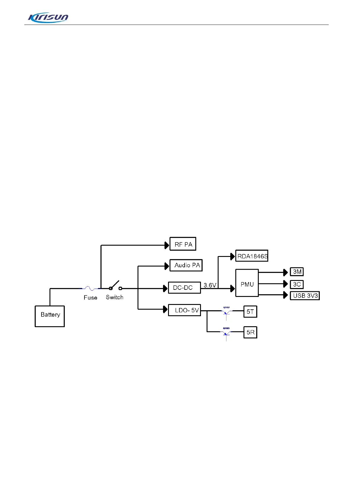
4.6.Power Section
The radio applies 7.4V lithium-ion battery for power supply. RF power amplification and audio power
amplification are directly powered by battery; the battery outputs 3.6V to supply power to PMU in AT1846S
and HS8861 through DC-DC switch; 3M, 3C and USB3.3V output from PMU separately supplies power to
other baseband circuits; the battery outputs 5V voltage through LDO and then outputs separate 5T and 5R
after control by Q100 and Q102.
RF PA: RF Power Amplifier Circuit Q500 (RD07MUS2B), Q501 (RD01MUS2)
Audio PA: Audio Power Amplifier Circuit U3 (TDA8547TS)
3M: EEPROM IC200 (AT24C512C)