FS-9120DN/9520DN
2-3-4
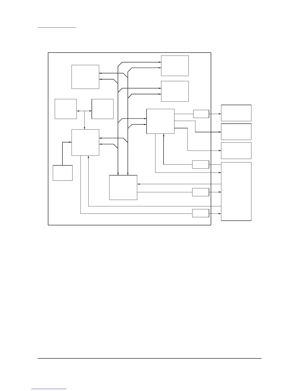
2-3-2 Engine controller PWB
Engine controller PWB
Printing data
Reset signal
Control signal output
Detection signal input
Control signal output
Detection signal input
Address bus
Data bus
Reset
circuit
U10
BUF
Driver
Control signal output
Detection
signal input
Tr
Driver
LSU
Main controller
PWB
High-voltage
transformer unit
Paper feeder
Drum unit
Developing unit
Fuser unit
Duplex unit
Saddle finisher*
Booklet stitcher*
*Optional.
CPU
U8
SRAM1
U9
SRAM2
U11
CPU
FLASH
U6
EEPROM
U13
EEPROM
U14
Engine G/A
U15
XIO
U16
Figure 2-3-3 Engine controller PWB block diagram
The engine controller PWB (EPWB) consists of the CPU. The CPU U8 communicates with other circuit boards, the image
processing system and the engine drive system.
The CPU U8 operates on an 8-bit bus. It uses the SRAM U9 and U11 for work memory. In accordance with the control
program in the program FLASH U6, the CPU U8 communicates with the optional devices via the serial communication
function in the CPU and XIO U16. The CPU U8 controls the LSU, which is for image output control via the image processing
engine G/A U15, and drives the machine, conveys paper and detects abnormalities via XIO U16.
 Loading...